Timing Verification of Dynamically Reconfigurable Logic for the Xilinx Virtex FPGA Series Ian Robertson, James Irvine, Patrick Lysaght*
David Robinson
Dept. Electronic and Electrical Engineering
Institute for System Level Integration
University of Strathclyde
The Alba Centre
204 George Street
Simpson Parkway
Glasgow, G1 1XW
Kirkton Campus
United Kingdom
Livingston, Scotland
+44 (0) 141 548 2250
EH54 7BH
[email protected] ABSTRACT
handcrafting to cover the conventional tools inadequacies.
This paper reports on a method for extending existing VHDL design and verification software available for the Xilinx Virtex series of FPGAs. It allows the designer to apply standard hardware design and verification tools to the design of dynamically reconfigurable logic (DRL). The technique involves the conversion of a dynamic design into multiple static designs, suitable for input to standard synthesis and APR tools. For timing and functional verification after APR, the sections of the design can then be recombined into a single dynamic system. The technique has been automated by extending an existing DRL design tool named DCSTech, which is part of the Dynamic Circuit Switching (DCS) CAD framework. The principles behind the tools are generic and should be readily extensible to other architectures and CAD toolsets. Implementation of the dynamic system involves the production of partial configuration bitstreams to load sections of circuitry. The process of creating such bitstreams, the final stage of our design flow, is summarized.
This paper introduces extensions to a previously reported CAD tool named DCSTech [2] which was created to automate the process of translating dynamic designs from VHDL into placed and routed circuits. The original version of the tool supported the Xilinx XC6200 family of FPGAs, and concentrated on the timing verification aspects of the problem. This paper reports on the extensions made to DCSTech to target the Xilinx Virtex family, and to enhance its capabilities. As a mainstream commercial FPGA, the design tool capabilities available with this family exceed those of the XC6200, allowing the designer to work more productively at a higher level of abstraction. By combining the Virtex platform’s capabilities with those of the extended DCSTech, the designer has the ability to specify designs in RTL/behavioural VHDL, place and route them and verify their timing. DCSTech’s back-annotation support has been extended to produce VITAL VHDL models suitable for DRL in addition to processing SDF timing information. This enables back-annotated timing analysis regardless of the level of abstraction at which the original design was produced.
Keywords Dynamic Reconfiguration, Run-Time Reconfiguration, FPGA, Verification.
1. INTRODUCTION In dynamically reconfigurable logic (DRL), a circuit or system is adapted over time. This presents additional design and verification problems to those of conventional hardware design [1] that standard tools cannot cope with directly. For this reason, DRL design methods typically involve the use of a mixture of industry standard tools, along with custom tools and some . Permission to make digital or hard copies of all or part of this work for personal or classroom use is granted without fee provided that copies are not made or distributed for profit or commercial advantage and that copies bear this notice and the full citation on the first page. To copy otherwise, or republish, to post on servers or to redistribute to lists, requires prior specific permission and/or a fee.
The original DCSTech tool was written to be extensible to other architectures. This work verifies the validity of its extensibility hooks. The extensibility of DCSTech to other architectures relies on the architecture’s CAD tools supporting a select set of capabilities. Most modern CAD tools meet the majority of these requirements (with the exception of configuration bitstream access), although some weaknesses, particularly in the control of routing, are apparent. Therefore, the design techniques presented here should be readily extensible to other dynamically reconfigurable FPGAs. The paper begins by reviewing existing work in section 2 before presenting the challenges of DRL design in section 3. In section 4 we provide an overview of the principles behind DCSTech while section 5 describes how they are applied to the Virtex. Section 6 discusses the enhanced back annotation capabilities necessary for design at the RTL and behavioral abstraction levels. The tools are designed to be as architecture independent as possible and section 7 describes how the tool may be extended
FPGA’02, February 24-26, 2002, Monterey, California, USA. Copyright 2002 ACM 1-58113-452-5/02/0002…$5.00.
*Now at Xilinx Inc.
to support other dynamically reconfigurable FPGAs. In section 8, we describe how partial configuration bitstreams may be obtained from the placed-and-routed subsections of the dynamic design, an area of current research. The design flow is illustrated with an example in section 9 before the paper concludes with remarks on future research into the use of other modern CAD techniques such as Static Timing Analysis (STA) within the DRL design flow.
2. EXISTING WORK Over the last six years, researchers have developed a number of tools and techniques, supporting different target DRL systems. The target systems can be characterized by their component set, the set of resources that make up the system. Custom Computing Machines (CCMs), for example, include processors, FPGAs and memory in their component set. Tools ranging from high-level language compilers to structural-level hardware/software co-design environments have been designed for such target systems. CCM compilers include tools such as Nimble [3], and compilers for the GARP chip [4], which compile ANSI-C. In addition to standard C compilation, CCM compilers partition the application into a software executable and a set of hardware modules that can be loaded onto the reconfigurable datapath or FPGA. As these tools are aimed at achieving a rapid design flow, similar to conventional computer programming, they do not usually achieve optimum results. Tools such as JHDL [5][6], a structural/RT level hardware/software codesign environment based on Java, allow the designer to customize his circuitry and specify its placement. This allows designers to use their own expertise to optimize the layout and composition of their circuits to achieve better results (e.g. faster circuits and smaller reconfiguration bitstreams if partial reconfiguration is used) as well as designing the associated software in one environment. Another design challenge is found when the component set is a single FPGA device or when dynamic reconfiguration is applied within individual devices. This sort of design throws up many situations that most industry standard tools cannot handle at all, such as verification, partial bitstream generation and automatic configuration controller production. Many of the solutions developed for this type of design also apply to CCM design. In [7], Luk et al described a CAD framework for DRL design targeted at the Xilinx XC6200 FPGA. A library based design approach was used to encourage design reuse and control circuit placement. This increases the similarity between successive configurations and reduces the size of the partial configuration files required. However, such a structural design approach limits the portability of the tools, since new libraries targeted to each device are required. Vasilko’s DYNASTY [8] CAD framework uses a designer driven temporal floorplanning approach, in which the designer can visualise the layout of tasks on the FPGA over time. It acts as a DRL-aware replacement to a place and route (PAR) tool and operates on synthesised gate-level designs. This has a number of advantages, such as ease of area estimation and the ability to control routing and component placement exactly. The designer therefore has the ability to generate exactly the required layouts. However, as the tools are closely
associated with the XC6200 architecture considerable effort would be required to port them to operate with other devices. Research has also taken place into the use of alternative languages that have useful properties in expressing aspects of a DRL design. Ruby [9], Pebble [10] and Lava [11] allow the designer to specify component placement using more convenient methods than the usual use of attributes associated with standard HDL designs. Pebble also includes a reconfigure-if statement, which builds in support for DRL. Recent work with Lava has seen it used with the Xilinx Virtex FPGA. The DCS CAD framework provides simulation (DCSim) [1], technology mapping and back annotation (DCSTech) [2] and configuration controller synthesis (DCSConfig) [12]. Although DYNASTY uses the same ideas as DCSTech, DCSTech partitions the design at a higher level of abstraction. This gives two advantages in the form of portability and circuit specialisation by the synthesis tool. Since the design is partitioned at an abstract level, DCSTech requires only a little device specific knowledge. The majority of the partitioning process is platform independent, as is the resulting circuit description. The tool is therefore easily ported to support different architectures. As the designs are synthesised after partitioning any optimisations such as constant propagation can be performed by the synthesis tools. If the design is partitioned after synthesis, a further optimization stage may be required to obtain the best results. At this level of abstraction the area requirements of the circuit are more difficult to estimate, so some iteration may be required to obtain the optimal layout. Other researchers have concentrated on design at lower levels of abstraction, allowing the designer absolute control over component placement and routing. Such tools include CHASTE [13], which provides access to the XC6200 configuration file and the JBits SDK [14][15], which provides a variety of tools to access, modify and verify Virtex configurations. In addition, it allows the designer to produce new whole or partial configurations. This approach could also be valuable as a method of performing final optimizations at the end of a higher-level design flow.
3. IMPLEMENTATION CHALLENGES DRL is based on a many-to-one temporal logic mapping. This means that different logic functions occupy the same area of the logic array at different points in time. Tasks that share physical resources cannot be active at the same time; they are mutually exclusive. Tasks can also be mutually exclusive for algorithmic reasons. A set of mutually exclusive tasks is called a mutex set and the swappable tasks are termed dynamic tasks. Tasks that are not altered in any way over time are described as static tasks. In designing a dynamic system, the various tasks must be placed in such a way as to ensure that no task is accidentally overwritten while it is active. The consequences of such an error range from subtle errors in operation to damage to the FPGA itself. Dynamic tasks are added to and removed from the array by loading partial configuration files to alter logic and routing. The designer has to guarantee that all necessary connections between the dynamic task and the surrounding environment will be made.
The routing paths configured onto the array with the dynamic task must meet the routing coming from the surrounding array to which they are intended to connect. The bitstreams must not cause contention, for example by configuring a second driver onto a bidirectional routing resource. The final problem the designer faces is that standard CAD tools, which are intended for the design of static circuits, will not accept the mapping of more than one function to a particular logic resource. Similarly, multiple drivers for a particular signal would be treated as an error, since no mechanism exists to indicate that the drivers are scheduled to operate at different times.
4.
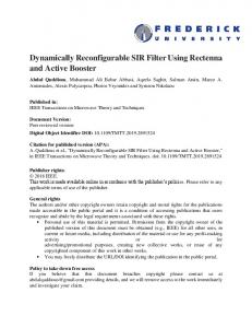
AUTOMATING DYNAMIC DESIGN PROCESSING WITH DCSTech 4.1 Overview DCSTech was designed as a tool to help the designer to overcome these problems. It can be thought of as a domain converter between the static and dynamic domains, fig. 1. The input dynamic system is split into a series of static designs on which conventional design tools (synthesis and APR) can be used. After the required implementation steps have been performed on these static sub-designs, a number of files are produced. VITAL compliant VHDL files that describe the systems functionality are created, along with SDF files specifying the circuit’s timing and configuration bitstreams. These files all require further processing before they are useful. To verify the designs functionality and timing, the SDF and VHDL files must be converted back to the dynamic domain, in order to simulate them in the context of the overall system. To implement the dynamic system, the configuration bitstreams must also be converted into valid partial reconfigurations. The original version of DCSTech supported the domain conversion of timing information. This was because designs were specified at the netlist level, and therefore a VITAL compliant simulation model could be produced from the original design. The use of higher design abstractions such as behavioural code combined with synthesis means that no such netlist exists before synthesis. The current version has therefore added netlist conversion to the static designs VHDL
original SDF conversion, leaving bitstream conversion as a manual process. The progress so far is illustrated in fig. 2.
4.2 Design and File Flow The dynamic design input to DCSTech consists of VHDL files describing the systems functionality. Each dynamic task is represented as a component instantiation. Hence, the top-level of the design is structural. Within each component, any synthesisable level of abstraction can be used. The designer assigns each dynamic task to a mutex set. This mutex set is assigned a zone on the logic array and all dynamic tasks within that set must reside within the corresponding zone. Thus, tasks within a mutex set can overwrite each other, but static logic and tasks in other mutex sets are unaffected. The correct system operation is then assured so long as an appropriate reconfiguration schedule is used (it is possible that the configuration control mechanism used to activate and deactivate tasks could cause problems if it is incorrectly designed). Clearly, the zone of each mutex set must be large enough to accommodate its largest task.
SDF
DCSTech
VHDL
Bitstream
Original Version
This Version
Future work
9
9
9
8
8
9
8
9
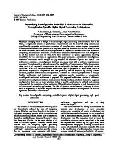
Figure 2: Domain transforms performed by different DCSTech versions The dynamic intent of the system is captured in a Reconfiguration Information Format (RIF) file. This file describes the conditions under which tasks activate (are configured onto the FPGA) and deactivate (are removed or stopped), the mutex set to which they belong and their placement. Information on the RIF file was published in [2]. In the static domain, one of the sub-designs deals with all the static tasks in the design while each dynamic task is placed into a static results
Conventional CAD Tools
dynamic timing results
Timing Model
VHDL Timing Model
DCSTech
DCSTech Reconfiguration Information
VHDL
Dynamic
Conventional CAD Tools
Static
9
Timing Model
Dynamic
Figure 1: DCSTech: Domain conversion between static and dynamic domains
floorplan of static-task design B A
A and D are static tasks B and C are mutually exclusive dynamic tasks
D C
A
Re se
rve
d
D
floorplan of a dynamic task B floorplan of dynamic design B
A
B
DCSTech
D
C floorplan of a dynamic task C Special terminals used to lock the ends of cut signals to a fixed position in the static-task design and in relevant dynamic task designs Dynamic
C
Static
Figure 3: Floorplan of a DRL circuit containing two dynamic tasks before and after processing by DCSTech sub-design of its own. The concept of terminals is used to ensure the correct routing connectivity with the dynamic tasks surrounding environment. These are special components used to lock the end of hanging signals to a particular location on the logic array. By locating both hanging ends of the signal at the same place, the connection can be easily produced. One reserved area is added to the static sub-design for each mutex set in the original design. Similarly, the dynamic task components are surrounded by a bounding-box that ensures that they will be placed within the reserved area for their mutex set, fig. 3. After the sub-designs have been placed and routed by standard back-end tools, accurate estimates of their timing can be made. These estimates are typically written out into an SDF file. To allow evaluation of the performance of the system, this information must be applied to the overall dynamic system. DCSTech is capable of mapping the SDF information into the dynamic design simulation model that DCSim creates, allowing timing simulation. To apply the SDF file to the dynamic domain, the cells must each be changed to match the hierarchy of the dynamic system simulation to which it is applied. In addition, the timing entries for the terminals are removed and their relevant timing information mapped to isolation switches (simulation artefacts added by DCSim to mimic the design’s dynamic behavior in a conventional simulator). Although the system hierarchy is altered during this domain conversion process, the actual timing information is unaltered, providing an accurate timing model. Further details of the process can be found in [2].
5.
CHANGES MADE TO DCSTech TO TARGET THE VIRTEX
A number of changes were required in order to retarget the static design representations to Virtex synthesis and APR tools, as
summarized in table 1. These changes allow us to replicate the capabilities DCSTech made available for the XC6200 on the Virtex. Table 1. Methods of implementing DCSTech requirements on XC6200 and Virtex Problem
XC6200 Solution
Virtex Solution
Reserving areas of the array
Reserve constraint
Prohibit constraint
Locating dynamic tasks within a zone
bbox attribute assigns a bounding box
loc constraint allows ranges to be assigned
Preventing partial circuits from being removed
Use register as terminal component on hanging signals
Changes to design representation and software settings
Lock hanging signals to fixed array locations
Terminal components with rloc constraints
Terminal components with loc constraints
Reserving areas on the logic array is a simple change of attribute from a RESERVE constraint which prevents XACT6000 from placing logic in the specified zone to specifying a PROHIBIT constraint which does the same task in the Xilinx CAD tools. This is added to the User Constraints Format (UCF) file. Dynamic task locations can be set using a combination of an rloc and a bbox attribute in XACT6000. The Virtex tools allow location ranges to be specified with the loc attribute. Because registers could be read from and written to through the XC6200 configuration interface, any line connected to and from registers was considered a valid connection, even when the
register had incomplete connectivity, such as no output connection. Using registers to terminate hanging nets therefore prevented partial circuits from being removed. This technique does not work with the Virtex synthesis tools, making two changes necessary in the way that dynamic designs were represented in the static domain. Firstly, the VHDL entity of each dynamic task must have ports in it to describe its connectivity, whereas before terminal components were all that was required. In addition, to prevent large areas of the static design being optimised away, the connectivity between the inputs and outputs of the reserved area should be indicated. Instantiating a black-box “mutex set” component, encapsulating the inputs and outputs of all the dynamic tasks in the mutex set solves this problem. The Xilinx Foundation tools support an option not to remove unconnected logic, which suffices for the placement and routing stage. The terminal component used to terminate hanging nets has been changed to a wire or buffer mapped to a look-up-table. This component replaces the RPFDs and FDCs used on the XC6200 and has an advantage in that it does not contribute any functionality, while accepting location constraints. This simplifies the changes required in the final bitstream generation stage and the netlist conversion process. The changes described above allow most of the basic requirements outlined in section 3 to be met by the standard Virtex tools. However, one area of weakness is constraining the placement of routing. The constraints described above only apply to logic placement, and therefore the routing from circuits can exceed their bounding boxes and invade reserved zones, although the Xilinx modular design tools [16] can help alleviate this problem. These are factors that the designer must take account of when configuration bitstreams are being produced, either by re-routing the offending lines, or by including the routes in the appropriate configurations. In effect, the dynamic task bounding-box should be increased in size to accommodate any wayward routing.
6. ENHANCED BACKANNOTATED TIMING SUPPORT The original static-to-dynamic domain conversion support for SDF files has been enhanced in the new revision of DCSTech. SDF information can only be applied to gate-level VITAL
Dynamic design domain Options
DCSim’s CRF file
RIF
VHDL
SDF
compliant designs. If a design is produced at an abstract level, then SDF information cannot be applied to it. As with most modern APR tools, the Virtex tools are capable of writing out a VITAL VHDL netlist that matches their SDF files. The netlists are typically flat “seas of gates” with no hierarchy (although many tools allow control over hierarchy flattening). These files must be included in the domain conversion process in order to allow timing analysis to be performed when design abstractions above the structural level are used. DCSTech handles this domain conversion process by instantiating the dynamic tasks into the VHDL netlist for the static design. The resulting dynamic circuit is, in effect a gate-level version of the original RTL design, such as a DRL aware synthesis tool might produce. DCSim is used to simulate the circuit. Since the hierarchy of the system often changes if synthesis and APR tools flatten the design, it may not match the hierarchy entries in the original RIF file. Therefore, a new RIF file is written as part of the domain conversion process. The domain conversion therefore produces a complete new dynamic design representation that DCSim can use to build a simulation model. As reported in section 4, the relevant timing information associated with the terminal components is usually applied to DCSim’s isolation switches while the references to the terminal components are removed from the design. However, the Virtex terminal components have no functionality and therefore do not interfere with the simulation of the system. As a result, those components that contribute timing data do not need to be removed during the static to dynamic domain conversion; hence, there is no need to retarget the timing data to the isolation switches (although the isolation switches are still introduced as they are needed to simulate the circuit). This simplifies the conversion process thereby reducing the runtime of the DCSTech tool.
7. THE EXTENDED DCSTech TOOL DCSTech now provides multi-architecture support and interfaces with several third party CAD tools. It was originally designed to be extensible with as much of the technique as generic and device independent as possible. Obviously, changes in the CAD environment and device architectures will mean that parts of the technique will need to be changed, either to take advantage of device features or to coexist with its supporting CAD
VITAL VHDL
Virtex dependent functions
DCSTech
CRF file Log file VHDL
SDF
XC6200 dependent functions
VITAL VHDL
Static design domain Figure 4: File flow for the extended DCSTech tool
Other device dependent functions
framework. The major changes came on the back annotation side, where support for VHDL domain conversion was added. However, this is not something that is specific to the Virtex device, but a necessary step to enable designers to work at higher levels of abstraction. Therefore, the concepts behind the tool remain generic and architecture independent and the design methodology, outlined in section 4, remains unchanged in this revision. To facilitate this extensibility, the device dependent functions are stored in dynamic link libraries. New devices can therefore be supported with the addition of a DLL. The file flow for DCSTech is shown in fig. 4. The shaded files represent non-design files used as part of DCSTech’s operation. The CRF files are cross-reference files used to store information such as terminal component connectivity and isolation switch locations (DCSim). The log file contains reports for the user. The options file can be used as an alternative to typing in command line switches. The design philosophy described in this paper will be able to provide DRL design support for any FPGA and CAD tool set provided it complies with the following requirements: •
The FPGA is dynamically reconfigurable
•
Synthesis or design translation from VHDL is available
•
A suitable component can be found to lock the ends of hanging nets to a particular location on the logic array
•
A method is available to prevent unconnected circuits being removed from the design
•
Components can be assigned a bounding-box constraining them to a location on the array
•
Areas of the array can be reserved, prohibiting other logic from being placed within that area
•
The APR tools produce back annotated VITAL VHDL and SDF files
•
The names of elements instantiated into the design in a structural manner are predictable within the SDF and VITAL VHDL models. Components generated by synthesis tools generally have unpredictable names, but structural components are usually named after their instantiation label and the hierarchy above them in the original design. DCSTech has to be able to find the terminal components that are added to the design in the dynamic-to-static conversion as part of the static-todynamic conversion after APR
•
The configuration file is open to modification, via an open file format or APIs such as JBits. This is not necessary for DCSTech itself, but would be necessary to modify the bitstreams in order to actually implement the system
Since most modern CAD packages fulfil these requirements, with the exception of bitstream access, support for the majority of modern dynamically reconfigurable FPGAs should be possible with only minor alterations in addition to those described in sections 5 and 6.
8. BITSTREAM GENERATION Conventional CAD tools can provide a configuration bitstream for each of the partial circuits produced by DCSTech’s dynamicto-static conversion process. As shown in fig. 3, the partial circuits consist of one configuration representing all the static circuits and a configuration for each dynamic circuit. The static circuits are connected to terminal components that lock the ends of floating connections to dynamic circuits in place. Similarly, floating connections to the static circuits within each dynamic task are locked in place by identically located terminals. These overlying terminal components must be converted to a connection between the two routes, by altering the configuration bitstream. Unless the tools are capable of producing partial configuration files, their output files represent a configuration of each partial circuit on an otherwise unconfigured FPGA. If these files were applied to the FPGA, they would blank out all the existing circuitry. For the system to operate correctly, however, only circuitry that shares resources with the partial circuit to be loaded should be disrupted when it is activated. The partial circuit configurations need to be converted to partial configurations, which reconfigure only the area occupied by a dynamic task within its mutex set zone. A further complication is caused by the lack of control over routing placement noted in section 5. It is possible that routing in a dynamic task will use the same line as routing in a static task. If the dynamic task is then configured onto the array, the routing conflict will cause errors in operation and possibly device damage. The designer must ensure that the routing resources used by each dynamic task are not shared by static tasks or dynamic tasks in other mutex sets. The target device configuration mechanism is another factor in the strategy used to produce partial configurations. The XC6200 allows individual parts of the logic array to be altered; therefore, only parts of the array in the dynamic task bounding-box need be considered. In the Virtex, however, reconfiguration takes place in columns. The smallest unit of configuration data that can be applied is a frame, which configures a subset of the resources in a column. Forty-eight frames are required to completely configure a column [17]. As a result, all the logic and routing in any column which makes up part of a dynamic task boundingbox must be included in the partial reconfiguration bitstreams. Therefore, any static logic or routing that overlaps these columns, must be included in the partial configuration bitstream of that dynamic task otherwise it could be overwritten. For devices that contain bidirectional routing resources, care must be taken not to configure a second driver onto a line during the course of a partial reconfiguration otherwise device damage may occur. One possible solution to this problem is to apply a deactivate configuration, which blanks out existing circuitry on part of the array, prior to loading a new dynamic task, but this would increase the reconfiguration interval. To prevent static circuit disruption, the deactivate configuration needs to contain any static logic within the reconfiguration zone. The generation of partial bitstreams for the Virtex device therefore consists of several steps. Firstly, all the routing
resources used by each partial circuit must be evaluated. JRoute [18], part of the JBits SDK includes functions that perform this step. The routing should then be checked for conflicts between circuits that can reside on the array concurrently. The physical bounding-box for each dynamic task (which includes both logic and routing) should then be determined and, from this, the area occupied by each mutex set. The circuitry to be reconfigured for each dynamic task therefore includes all logic and routing within all the columns occupied by the mutex set area. In the Virtex FPGA, the terminal components can be converted to connections, simply by connecting the routes to both sides of the LUT (i.e. merging the routing to and from the two overlapping terminals). This is because the LUT is configured to behave like a wire. Once these processes have been completed, partial bitstreams for the affected FPGA areas can be generated (possibly including deactivate configurations). JBits includes support for this process via JRTR [15].
9.
The set of four multipliers therefore forms a dynamic task. One dynamic task is required for each coefficient supported. As the different coefficients are mutually exclusive, the dynamic tasks are all members of the same mutex set and can be assigned the same area of the logic array. Since the registers and adders surrounding the dynamic multipliers are not altered during the reconfigurations, they constitute its static circuitry. Based on these assignments, DCSTech can partition the dynamic design into multiple static designs that can be placed and routed as shown in fig. 1.
EXAMPLE COMPLEX NUMBER MULTIPLIER
As a simple example to demonstrate the operation of DCSTech, a dynamically reconfigurable constant complex number multiplier is presented. Complex numbers consist of two parts: the real part and the imaginary part, which is a coefficient of j (the square root of –1). The product of two complex numbers is calculated as follows:
p _ real = a _ real × b _ real − a _ imag × b _ imag p _ imag = a _ real × b _ imag + a _ imag × b _ real where p_real and p_imag are the real and imaginary parts of the product, p, of complex numbers a and b. The operation therefore requires four multipliers, an adder and a subtractor.
Figure 6. Post-APR layout of the 10+j12 dynamic task. This comprises the four multipliers shown in fig. 5, surrounded by terminal components. The areas highlighted in gray indicate terminal components, while the area highlighted in white indicates the dynamic task bounding-box
In the example, the complex product is formed by multiplying the input complex number, x, by a constant complex coefficient. The constant coefficient values can be hardwired into constant coefficient multipliers potentially saving area and improving performance. A diagram of the system, with a coefficient of 10 + j12, is presented in fig. 5. The constant complex coefficient is dependent on the multiplication factors of the four multiplier circuits. Therefore, to support a different coefficient, the four constant coefficient multipliers need to be changed. x_real
D Q
x_imag
X10
D
X12
D
X10
D
X12
D
Q
-
D
+
D
D Q
Q
p_real
Q
p_imag
Q
Q
Q
Figure 5. Circuit to multiply by 10+j12 The multipliers can be reconfigured to alter their multiplication factor and thus allow the system to support other coefficients. The remaining circuitry does not require alteration in any way.
Figure 7. Layout of the complex multiplier’s static circuitry. This consists of the registers, adder and subtractor in fig. 5, with terminal components locking the ends of connections to and from the multipliers in place. A complex multiplier with two dynamic tasks allowing multiplication by the coefficients (10 + j12) and (15 + j14) was created. The layout of the (10 + j12) dynamic task and the static circuitry after APR on a XCV50 is shown in figs. 6 and 7. Fig. 6
n_Rst Clk CE x_real x_imag p_real p_imag 10+j12Status 15+j14Status
Figure 8. A backannotated timing simulation waveform for the dynamically reconfigurable complex multiplier
shows evidence of routing exceeding the dynamic task’s bounding-box. Similarly, fig. 7 shows that some of the static circuit’s routing has been placed within the bounding-box. When implemented, the partial configuration bitstreams should include such stray routing as discussed in section 8. After APR, the circuits timing can be verified. DCSTech is used to reassemble the static parts of the system into a VITAL compliant gate-level model of the dynamic system and create a matching SDF file. A new RIF file is written as part of this process, to match any design hierarchy changes which occurred during synthesis and APR. This model is then further processed by DCSim to produce a dynamic simulation model, making use of the new RIF file. A waveform for the timing simulation of the system is shown in fig. 8. The input number is represented by x_real and x_imag and is set to 15 + j16. At 110 ns, the n_Rst (reset) input is de-asserted, allowing the multiplier to begin operation. The two status signals at the bottom of fig. 8 indicate the configuration status of the two dynamic tasks. Initially, task 15 + j14 activates. The first multiplication is therefore:
(15 + j16) × (15 + j14) , which equals (1 + j450), matching the result displayed on the outputs p_real and p_imag after 200 ns. At 240 ns task 10 + j12 activates. For simplicity, a time of 50 ns is assumed for the reconfiguration. Two clock edges occur during the reconfiguration interval. The exact configuration of the mutex set zone is uncertain during this time. The simulation model therefore puts ‘X’ on all the dynamic task outputs during this period. These can be seen emerging from the pipeline between 290 and 355 ns. Thereafter, the result of multiplication by (10 + j12), which is (-42 + j340), is displayed on the p output.
These tools can read a variety of file formats including VHDL and SDF. Since the new version of DCSTech produces both these files, it therefore may enable the application of STA to the dynamic design. While this would not take into account the time consumed by reconfigurations, it would allow the verification of all the timing issues that affect circuit performance, such as maximum clock speed, critical path and set-up and hold times. In the DRL design flow presented in this paper, the designer is faced with the problem of partitioning the design at the RT level, rather than a lower level of abstraction. At this level, the exact area occupied by each block is unknown, although it can be estimated approximately. Therefore, some iteration and refinement may be required to obtain a suitable partitioning. A design management tool could simplify this process, by estimating area requirements for each task in the application and presenting the information graphically. Temporal floorplanners for netlists have already been developed. This would be a similar idea but at a higher level of abstraction. Most of the bitstream generation steps outlined in section 8 are currently carried out manually. As the APIs in JBits carry out many of the more complex functions associated with Virtex partial bitstream generation, it is possible to automate the process and this is the focus of future work.
11. CONCLUSIONS
10. FUTURE WORK
This paper shows how the major similarities between the standard CAD tools available for different FPGA architectures can be exploited to implement an easily portable CAD framework for DRL design. The technique relies on a select set of capabilities, supported by most CAD toolsets, within the underlying FPGA platform’s supporting tools. From this, automated support for the main stages of the DRL design flow can be provided, including design specification, simulation, synthesis, APR and timing extraction.
For large systems, the use of timing simulation to verify timing is a slow process. Not only does the simulator require long runtimes, but also a lot of effort is required to generate a testbench with sufficient test-vectors and coverage. Static Timing Analysis (STA) is a timing verification approach that evaluates the timing of each path through the circuit without test-vectors.
The final stage of the design flow is partial bitstream generation. The ideas behind partial bitstream generation, which are common across different FPGA families, were outlined. However, the exact method used to produce these bitstreams depends on both the capabilities of the standard CAD tools and the FPGA’s configuration interface. The broad similarities
evident in the standard CAD tool support for most platforms are not replicated at this level. Indeed, most vendors provide no mechanism for accessing configuration bitstreams at all, since this compromises design security. As a result, bitstream generation techniques will not port well between families. For the Virtex, however, the availability of the JBits SDK provides convenient access to its bitstream along with a number of functions useful in bitstream generation.
12. REFERENCES [1] D. Robinson and P. Lysaght, “Verification of Dynamically Reconfigurable Logic”, in Field Programmable Logic and Applications, R. Hartenstein and H. Grunbacher (Eds), pp. 141 – 150, Villach, Austria, August 2000.
[2] D. Robinson and P. Lysaght, “Methods of Exploiting
[8] M. Vasilko, “DYNASTY: A Temporal Floorplanning Based CAD Framework for Dynamically Reconfigurable Logic Systems”, in Field Programmable Logic and Applications, P. Lysaght, J. Irvine and R. Hartenstein (Eds), pp 124 – 133, Glasgow, UK, August 1999.
[9] J. Hogg, S. Singh and M. Sheeran, “New HDL Research Challenges posed by Dynamically Reprogrammable Hardware”, The Third Asia Pacific Conference on Hardware Description Languages, Bangalore, India, January 1996.
[10] W. Luk and S. McKeever, “Pebble: A Language for Parameterised and Reconfigurable Hardware Design”, Field Programmable Logic and Applications, R. Hartenstein and A. Keevallik (Eds.), Tallin, Estonia, September 1998.
Simulation Technology for Simulating the Timing of Dynamically Reconfigurable Logic”, IEE ProceedingsComputers and Digital Techniques 147: (3) 175-180 May 2000.
[11] S. Singh and P. James-Roxby, “Lava and JBits: From HDL
[3] Y. Li, T. Callahan, E. Darnell, R. Harr, U. Kurkure and J.
Configuration Controllers for Dynamically Reconfigurable Logic Systems Using the DCS CAD Framework”, in Field Programmable Logic and Applications, P. Lysaght, J. Irvine and R. Hartenstein (Eds), pp. 41 - 50, Glasgow, UK, August 1999.
Stockwood, "Hardware-Software CoDesign of Embedded Reconfigurable Architectures", 37th Design Automation Conference, Los Angeles, USA, June 2000.
[4] T. J. Callahan, J. R. Hauser, and J. Wawrzynek, “The GARP Architecture and C Compiler”, Computer, Volume 33, Issue 4, pp. 62 – 69, April 2000.
[5] P. Bellows and B. Hutchings, “JHDL-An HDL for Reconfigurable Systems”, in Proceedings of the IEEE Symposium on Field-Programmable Custom Computing Machines, Napa, California, April 1998.
[6] M. J. Wirthlin, B. L. Hutchings and C. Worth,
to Bitstreams in Seconds”, IEEE Symposium on FPGAs for Custom Computing Machines, April 2001.
[12] D. Robinson and P. Lysaght, “Modelling and Synthesis of
[13] G. Brebner, “CHASTE: a Hardware/Software Co-design Testbed for the Xilinx XC6200”, Reconfigurable Architectures Workshop, Geneva, Switzerland, April 1997.
[14] S. Guccione, D. Levi and P. Sundararajan, “JBits: Java based interface for reconfigurable computing”, Military and Aerospace Applications of Programmable Devices and Technologies Conference, 1999.
“Synthesizing RTL Hardware from Java Byte Codes”, in Field Programmable Logic and Applications, G. Brebner and R. Woods (Eds), pp. 123 – 132, Belfast, Northern Ireland, UK, August 2001.
[15] S. McMillan and S. Guccione, “Partial Run-Time
[7] W. Luk, N. Shirazi and P.Y.K. Cheung, “Compilation
[16] Xilinx Inc., “Xilinx Alliance 3.1i Modular Design”, version
Tools for Run-Time Reconfigurable Designs”, in Proc. IEEE Symposium on Field-Programmable Custom Computing Machines, K.L. Pocek and J. Arnold (editors), pp. 56 - 65. 1997.
Reconfiguration Using JRTR”, in Field Programmable Logic and Applications, R. Hartenstein and H. Grunbacher (Eds), pp. 352 – 360, Villach, Austria, August 2000. 1.2, April 20, 2001.
[17] Xilinx Inc., “Virtex Series Configuration Architecture User Guide”, version 1.5, Sept. 27, 2000.
[18] E. Keller, “JRoute: A Run-Time Routing API for FPGA Hardware”, 7th Reconfigurable Architectures Workshop (RAW2000), Cacun, Mexico, May 2000.