PROOF COPY 006410JES
Journal of The Electrochemical Society, 151 共10兲 1-0 共2004兲
1
0013-4651/2004/151共10兲/1/5/$7.00 © The Electrochemical Society, Inc.
Electrical Characteristics of Thermally Evaporated HfO2 R. Garg,a N. A. Chowdhury,a M. Bhaskaran,b P. K. Swain,b and D. Misraa,*,z a
Department of Electrical and Computer Engineering, New Jersey, Institute of Technology, Newark, New Jersey 07102, USA b Sarnoff Corporation, Princeton, New Jersey 08543-5300, USA
O PR
The electrical characteristics of hafnium oxide (HfO2 ) films, grown by standard thermal evaporation of hafnium while adding oxygen at constant partial pressure during evaporation, were investigated for the first time. The dielectric constant as measured by the capacitance-voltage technique is estimated to be in the range of 18-25. Metal oxide semiconductor 共MOS兲 capacitors using HfO2 as dielectric and annealed at 450°C show a hysteresis below 30 mV. A low leakage current density of ⬍10⫺7 A/cm2 at 1 V and reduced bulk oxide charges 1.61 ⫻ 1011/cm2 were also observed. The interface state density and low-temperature charge trapping behavior of these films were also investigated. Observed characteristics indicate that HfO2 films deposited by standard thermal evaporation are suitable for MOS device applications. © 2004 The Electrochemical Society. 关DOI: 10.1149/1.1784212兴 All rights reserved. Manuscript submitted November 18, 2003; revised manuscript received February 17, 2004.
OF
Hafnium oxide (HfO2 ) has been under intense investigation recently for replacing conventional SiO2 共or SiOx Ny ) as a high dielectric constant 共high-k兲 gate dielectric in complementary metal oxide semiconductor 共CMOS兲 devices to reduce tunneling current and boron penetration.1 Even though many high-k materials are currently being studied, poor short channel effects due to the fringing field induced barrier lowering effect2 and thermal instability due to the formation of silicides or interfacial layers impede the effectiveness of these materials when directly in contact with silicon.3 An HfO2 film has a high dielectric constant 共⬃25兲, high heat of formation 共271 kcal/mol兲, and a large bandgap 共5.68 ev兲,4,5 and is thermally stable when in contact with silicon. In addition, HfO2 is compatible with n⫹ polysilicon without any barrier layer.6 Various methods, such as atomic layer deposition,7 evaporation with ion-assisted deposition,8 sputtering,9 in situ rapid thermal chemical vapor deposition,10 and reactive electron beam evaporation11 have been explored to deposit reliable and high-quality HfO2 thin films. The properties of the grown film and interface show a pronounced dependence upon the deposition process and the precise deposition parameters chosen. Each technique has its own set of advantages and disadvantages. However, most of these techniques show some kind of interface damage. Sputtering and E-beam assisted depositions create radiation induced surface damage during film growth. Therefore, all these techniques require high-temperature annealing, which results in further deterioration of device performance and reliability. Because the HfO2 -Si interface is critical for excellent device characteristics, it is important to investigate other reliable deposition techniques for a high-quality interface. In this work, HfO2 thin films were deposited, for the first time, by a standard thermal evaporation technique while adding oxygen at constant partial pressure during evaporation. Thermal evaporation doesn’t produce much damage to the interface, and it doesn’t require high-temperature processing in comparison to the other techniques mentioned previously. Electrical characteristics of HfO2 films have been studied using MOS capacitors. To investigate the charge trapping characteristics of HfO2 films, a low-temperature characterization was done.
PY
CO
pressure in the chamber increased to 10⫺4 Torr. Tungsten boats were used in evaporating the hafnium. The films were deposited at room temperature. However, the measured substrate temperature was around 30-35°C because of source-induced substrate heating. No residual gas analysis was performed during evaporation. Immediately before the deposition of the films, the wafers were cleaned by the standard RCA clean 共RCA-1 and RCA-2兲 followed by a 50:1 HF dip for 15 min. After the deposition of the HfO2 film, a layer of 400 nm aluminum was deposited on top of the oxide film. Capacitors of various sizes were patterned by photolithography. Samples were subjected to post metal deposition annealing 共PMA兲 at 350 and 450°C for 20 min in forming gas anneal 共FGA: N2 /H2 5%兲. HfO2 film thicknesses of 50 and 60 nm were measured by ellipsometer after the deposition. Using the known physical thickness of the HfO2 film, the dielectric constant was measured using accumulation capacitance. High-frequency capacitance-voltage 共C-V兲 measurements and current-voltage measurements were performed using a Boonton 7200 capacitance meter and an HP4156B semiconductor parameter analyzer, respectively. The interface state density was estimated using the Terman method.12 A CTI Cryogenics M22 closedloop helium cooled refrigeration system and a Palm Beach Cryophysics model 4075 temperature controller were used for the lowtemperature measurements.
E-mail:
[email protected]
PROOF COPY 006410JES
The dielectric constant, estimated from electrical measurements, is in the range of 18-25. Table I11,13-16 shows the dielectric constant obtained by thermal evaporation compared with the dielectric constants obtained for HfO2 films by other techniques. It seems that the dielectric constant for thermally evaporated films is the highest. The lower values of effective dielectric constants for the HfO2 gate stack formed by other techniques are attributed to the interfacial layer thickness between the silicon substrate and HfO2 after post deposition anneal.11,17 If there is a growth of thin SiO2 layer at the HfO2 and silicon interface, then a noticeable reduction in depletion capacitance is observed. This occurs because the effective oxide thickness is estimated from the two capacitances 共interfacial layer and high-k layer兲 in series. The high dielectric constant of our thermally evaporated HfO2 films could be attributed to a lack of interfacial layer, as our samples were not subjected to a high-temperature anneal. A partial condensation of the HfO2 film may be possible, because an increased accumulation capacitance was observed after annealing.17 In addition, there may be possible tungsten contamination from the tungsten boats used in evaporating hafnium, which is currently being investigated further. Figure 1 shows the normalized C-V characteristics of the 50 nm HfO2 film at various annealing temperatures. An ideal C-V curve, determined by calculating the differential capacitance across the MOS gate stack between the experimentally measured accumulation
ES
z
J 10
* Electrochemical Society Active Member.
64
HfO2 films of two different thicknesses were deposited on n-type 共resistivity of 10-20 ⍀-cm兲 具100典 Si wafers by standard thermal evaporation. Oxygen was added at constant partial pressure during evaporation. The base pressure was maintained at 10⫺6 Torr before oxygen was added. As oxygen was added during evaporation, the
00
Experimental
Results and Discussion
PROOF COPY 006410JES
Journal of The Electrochemical Society, 151 共10兲 1-0 共2004兲
2
Table I. Dielectric constant comparison with other current techniques.
Film deposition techniques Thermal evaporation Electron beam evaporation11 Sputtering13 Atomic layer deposition14 Remote plasma oxidation15 Plasma enhanced CVD16
Lowest dielectric constant
Highest dielectric constant
18 18 18 16 19 14
25 22 21 23 19 16
O PR
OF
capacitance and the silicon depletion capacitance as a function of gate voltage,18 was also plotted in Fig. 1. For these measurements, Al gate MOS capacitors with an area of 1.26 ⫻ 10⫺3 cm2 were used. Measurements were taken before annealing as well as after 350 and 450°C FGA annealing. The C-V curves show a reduction in hysteresis up to 30 mV after 350°C anneal in comparison to the as-deposited film. No significant improvement was seen in hysteresis characteristics after 450°C anneal, though the curve was shifted toward the left, indicating a negative shift in flatband voltage. The reduction in hysteresis indicates the reduced charge trapping under negative gate bias. Partial passivation of interface states was possibly achieved as a result of FGA. As no reduction in oxide capacitance was observed after 450°C annealing, it is believed that an Al2 O3 -like layer or SiO2 layer could have formed at the aluminumHfO2 interface and silicon-HfO2 interface, respectively, during PMA. Partial condensation of HfO2 is also possible because of annealing. The observed combined effect shows an increase in net capacitance 共inset Fig. 1兲 suggesting minimum impact of the interfacial layer. Comparison of experimental C-V curves with the ideal C-V curve 共no oxide charge兲 shows that the experimental C-V curve has moved closer to the ideal curve, indicating a reduction in bulk oxide charge from 6.97 ⫻ 1011/cm2 before annealing to 1.61 ⫻ 1011/cm2 after 450°C annealing. The high value of oxide charge (⬃1011/cm2兲 indicates a significant contribution from the interface-
trapped charge. The observed C-V stretch-out near inversion capacitance after 450°C annealing supports the presence of a high density of interface states. The C-V characteristics for the 60 nm HfO2 film are shown in Fig. 2. After 350°C anneal, hysteresis was reduced compared to the as-deposited films, but the stretch-out near inversion capacitance (C min) indicates that significant charge trapping remains at the interfacial region near the Si substrate. After 450°C annealing, the C-V curves are more symmetric for the voltage sweep, indicating a partial passivation of interface states. The inset in Fig. 2 suggests that some condensation of HfO2 has also occurred for the 60 nm films. Hysteresis was reduced to less than 175 mV, but is still much higher than that for the 50 nm HfO2 film 共Fig. 1兲. In addition, when the experimental C-V curves were compared with the ideal C-V curves, an increase in bulk oxide charges from 8.72 ⫻ 1011/cm2 before annealing to 1.15 ⫻ 1012/cm2 after 450°C annealing is noticed. This increase in oxide charge in 60 nm HfO2 could be due to stoichiometric defects or extensive interface defects, as the C-V curves in Fig. 2 have moved farther away from the ideal curve after 450°C annealing. Therefore, the characteristics show that 50 nm HfO2 films are electrically better than 60 nm thermally evaporated HfO2 films. To further investigate the oxide charge, the flatband voltage shift (⌬V FB) was plotted as a function of annealing, as shown in Fig. 3. For the 50 nm HfO2 film, ⌬V FB decreased from 1.1 V before annealing to 0.01 V after 450°C annealing, while for 60 nm thick hafnium oxide, ⌬V FB increased from 0.04 V before annealing to 0.8 V after 450°C annealing. One of the possible reasons for this behavior in 60 nm HfO2 films could be due to higher built-in stress during the deposition of HfO2 films, in comparison to the 50 nm film. Built-in stress generates bulk oxide defects as well as interface defects after the annealing of the films. The effect of annealing on the interface state density of these MOS capacitors is shown in Fig. 4. The Terman method was employed to estimate the interface trap density. Even though the Terman method has limited accuracy, it provides a quick estimate of interface trap density. The increase in interface state density was observed in both cases as a result of annealing. For the 50 nm HfO2 , it increased from 0.706 ⫻ 1012/cm2
PY
CO
Figure 2. Normalized C-V curves of MOS capacitors with 60 nm HfO2 film. Hysteresis of 175 mV can still be seen after 450°C annealing. When compared to ideal C-V curve, bulk oxide charges were increased to 1.15 ⫻ 1012/cm2, and interface state density was increased to 6.47 ⫻ 1012/cm2 eV after a 450°C anneal. The inset shows the absolute capacitance behavior for 60 nm devices.
ES
J 10
64
00
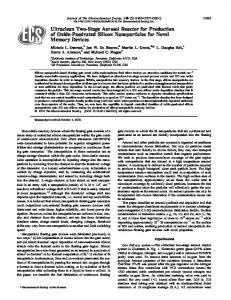
Figure 1. Normalized C-V curves of MOS capacitors with 50 nm HfO2 film. Hysteresis was reduced to 30 mV after 450°C annealing. When compared to the ideal C-V curve, bulk oxide charges were reduced to 1.61 ⫻ 1011/cm2, and interface state density was 1.75 ⫻ 1012/cm2 eV after samples were annealed at 450°C. The inset shows the absolute capacitance behavior for 50 nm devices.
PROOF COPY 006410JES
PROOF COPY 006410JES
Journal of The Electrochemical Society, 151 共10兲 1-0 共2004兲
O PR
OF
Figure 3. Effect of annealing on flatband voltage shift. In 50 nm HfO2 films, ⌬V FB has reduced from 1.1 to 0.01 V; in 60 nm HfO2 films, it has increased from 0.04 to 0.8 V.
Figure 5. Leakage current density in 50 and 60 nm HfO2 film MOS capacitors after 350°C and 450°C annealing.
but it was lower in the 50 nm films in comparison to the 60 nm ones. The observed improvement in leakage current in the 50 nm film is possibly due to the partial passivation of dangling bonds at the Si-HfO2 interface, as noticed from the C-V characteristics. However, in the 60 nm films, the leakage current becomes resistive around 1 V, indicating a large increase of interface states after 450°C annealing. To further understand the mechanism of leakage current through the dielectric, we have plotted ln(JFN /E 2ox) vs. 1/E ox in Fig. 6. The current due to Fowler-Nordheim 共FN兲 tunneling at sufficiently high electric field E ox follows the relationship given below19
PY
CO
eV before annealing to 1.75 ⫻ 1012/cm2eV after 450°C annealing, whereas for the 60 nm HfO2 , it increased from 2.2 ⫻ 1012/cm2 eV before annealing to 6.47 ⫻ 1012/cm2 eV after 450°C annealing. The increase in interface trap density can attributed to formation of a poor-quality interfacial layer. The significant degradation of interface quality in 60 nm HfO2 films could be due to the relaxation of the stress after annealing. The effect of annealing on the leakage current density of 50 and 60 nm HfO2 films is shown in Fig. 5. The leakage current density was decreased by more than two orders of magnitude after 450°C annealing in comparison to 350°C annealing in both of the HfO2 films. The leakage current density of the 50 nm HfO2 films was reduced to ⬍10⫺7 A/cm2 at 1 V after 450°C annealing. The leakage current density of 60 nm HfO2 was reduced after 450°C annealing,
3
ln共 J FN /E 2ox兲 ⫽ ln共 A 兲 ⫺ B/E ox
00
64
where J FN is the density of the FN current, and A and B are constants for a particular insulating film. From Fig. 5, E ox was calculated using the following equation19 E ox ⫽ V ox /t ox ,
V ox ⫽ V G ⫺ V FB ⫺ s
ES
PROOF COPY 006410JES
关2兴
where s is the surface potential at different positive bias voltages. The surface potential was estimated by comparing ideal and experimental C-V curves of the above mentioned MOS devices.12 Considering the effective mass of the electron at the HfO2 film to be 0.1m 0 , 20 we find that for t ox ⫽ 60 nm, ⌽ B ⫽ 0.3 eV and for t ox ⫽ 50 nm, ⌽ B ⫽ 0.43 eV when 1/E ox ⬎ 9 ⫻ 10⫺7 共cm/V兲 and ⌽ B ⫽ 0.28 eV when 1/E ox ⬍ 9 ⫻ 10⫺7 共cm/V兲. Here ⌽ B is calculated from slope B of the FN plots, which is equal to 6.83 ⫻ 107 ((m ox /m)⌽ B3) 1/2 共V/cm兲. The difference in effective barrier height is due to repairing of defects discrepancies. A straight line in Fig. 6b for the 60 nm film as predicted by Eq. 1 infers that at a high oxide electric field FN tunneling is the dominant leakage mechanism. However, the 50 nm film 共Fig. 6a兲 shows the same FN tunneling characteristics at high fields, but at low fields some improvement in trap assisted tunneling is evident. Because the 50 nm HfO2 films have shown better device performance in comparison to the 60 nm HfO2 films, we have investigated the charge trapping characteristics of 50 nm films at various temperatures. MOS capacitors with 50 nm HfO2 films of area 1.96 ⫻ 10⫺3 cm2 were studied. The temperature was gradually decreased from 290 to 130 K and high-frequency C-V measurements were taken once the sample attained a stable temperature. C-V curves at different temperatures 共see Fig. 7兲 demonstrated both parallel shift and stretch-out along the bias axis as the temperature was decreased. This verifies the presence of a higher number of both
J 10
Figure 4. Effect of annealing on interface state density. In 50 nm HfO2 films, it increased from 0.706 ⫻ 1012/cm2 eV before annealing to 1.75 ⫻ 1012/cm2 eV after 450°C annealing, whereas in 60 nm HfO2 films, it increased from 2.2 ⫻ 1012/cm2 eV before annealing to 6.47 ⫻ 1012/cm2 eV after 450°C annealing.
关1兴
PROOF COPY 006410JES
4
Journal of The Electrochemical Society, 151 共10兲 1-0 共2004兲
OF
O PR Figure 6. ln(JFN /E 2ox) vs. 1/E ox plot for Al/HfO2 /n-Si MOS capacitors with 共a兲 50 nm of HfO2 and 共b兲 60 nm of HfO2 .
charge is the only variable observed when the temperature was reduced. Considering the one-dimensional distribution of trapped charges along the oxide thickness, the oxide charge centroid can be defined as23
PY
CO
shallow bulk oxide and interface trapped charges at low temperatures. Electron trapping seems to be dominant because the higher barrier for holes in HfO2 共3.4 eV兲 compared to electrons 共1.5 eV兲21 enhances the electron trapping probability.21 The electron traps, especially shallow bulk oxide ones with energy levels close to the conduction band, became more active as the temperature went down, and this contributed to the shift of the C-V curves at low temperatures.22 Moreover, we can observe hysteresis above the midgap voltage in the C-V curves at low temperature. The flatband voltage shift (⌬V FB) was calculated for the devices under test at different temperatures. Figure 8 shows the ⌬V FB for some samples at temperatures ranging from 290 to 130 K. A turnaround effect was observed in ⌬V FB , as it increased initially when the temperature was decreased to 210 K and then it started to decrease when the temperature was decreased further to 130 K. To explain this turnaround effect in ⌬V FB , the concept of a trapped charge centroid model was used.21 In these devices, oxide
q
冕
tox
0
x 共 x 兲 dx ⫽ qN t⫺equiv • x t
关3兴
ES
J 10
64
00
where (x) is the trapped charge distribution function, t ox is the oxide thickness, and N t⫺equiv is the equivalent trapped charge per unit area having a centroid at x t . Here, trapped charges consist of both interface and oxide trapped charges, and x t ⫽ 0 at the gate and x t ⫽ t ox at the substrate. It is obvious from Eq. 1 that the density, location, and polarity 共positively charged/negatively charged兲 of individual traps affect the location of the centroid. Considering only the contribution of trapped charges in ⌬V FB , 23 we get
Figure 7. Low-temperature C-V curves for 50 nm HfO2 MOS capacitor.
PROOF COPY 006410JES
Figure 8. Flatband voltage shift as a function of temperature for 50 nm HfO2 MOS capacitor. The inset shows the energy diagram for Al/HfO2 /n-Si, indicating a shift of the centroid toward the gate electrode.
PROOF COPY 006410JES
Journal of The Electrochemical Society, 151 共10兲 1-0 共2004兲
5
gate in the 210-130 K range, which subsequently shifted the trapped charge centroid toward the substrate and gate, respectively, may be the principal cause behind the turnaround effect in ⌬V FB . Conclusions
O PR
Figure 9. Interface states, D it , as a function of temperature for various Al/HfO2 /n-Si MOS samples measured by conductance method.
⌬N t⫺equiv xt • C ox t ox
OF
⌬V FB ⫽ ⫺q
Electrical characteristics of MOS capacitors with thermally evaporated HfO2 films have been reported. Characteristics such as hysteresis, leakage current density, and flatband voltage shift significantly reduced after 450°C FGA anneal in 50 nm HfO2 films. Bulk oxide charges decreased after annealing in 50 nm HfO2 films, whereas they increased for 60 nm films. The interface state density is toward the higher side and moderately increased with annealing. Furthermore, shifts in C-V curves and the turnaround effect in flatband voltage shifts were observed in the 290-130 K temperature range, giving the charge trapping characteristics of HfO2 films. Even though the films studied in this work are thicker than the thickness required for nanoscale device applications, the electrical properties investigated here suggest that thermally evaporated HfO2 films can be suitable for MOS device applications with enhanced process optimization.
关4兴
This work was supported by a grant from the National Science Foundation 共award no. ECS-0140584兲. The New Jersey Institute of Technology assisted in meeting the publication costs of this article.
References 1. The International Technology Roadmap for Semiconductors, 2001 ed., International Sematech, Austin, TX 共2001兲. 2. B. Cheng, M. Cao, R. Rao, A. Inain, P. V. Voorde, W. M. Greene, J. M. C. Stork, Z. Yu, P. M. Zeitzoff, and J. C. S. Woo, IEEE Trans. Electron Devices, 46, 1537 共1999兲. 3. T. J. Hubbard and D. G. Scholm, J. Mater. Sci., 11, 2757 共1996兲. 4. G. D. Wilik, R. M. Wallace, and J. M. Anthony, J. Appl. Phys., 89, 5243 共2001兲. 5. E. P. Gusev, D. A. Buchanan, E. Cartier, A. Kumar, D. DiMaria, S. Guha, A. Callegari, S. Zafar, P. C. Jamison, D. A. Neumayer, M. Copel, M. A. Gribelyuk, H. Okorn-Schmidt, C. D’Emic, P. Kozlowski, K. Chan, N. Bojarczuk, L.-A. Ragnarsson, P. Ronsheim, K. Rim, R. J. Fleming, A. Mocuta, and A. Ajmera, Tech. Dig. Int. Electron Devices Meet., 2001, 451 共兲. 6. B. H. Lee, L. Kang, W.-J. Qi, R. Neih, Y. Jeon, K. Onishi, and J. C. Lee, Tech. Dig. - Int. Electron Devices Meet., 1999, 133 共兲. 7. J. Aarik, A. Aidla, H. Mandar, T. Uustare, K. Kukli, and M. Schuisky, Appl. Surf. Sci., 173, 15 共2001兲. 8. M. Gilo and N. Croitoru, Thin Solid Films, 350, 203 共1999兲. 9. B. H. Lee, L. Kang, R. Neih, W.-J. Qi, and J. C. Lee, Appl. Phys. Lett., 76, 1926 共2000兲. 10. S. J. Lee, H. F. Luan, W. P. Bai, C. H. Lee, T. S. Jeon, Y. Senzaki, D. Roberts, and D. L. Kwong, Tech. Dig. - Int. Electron Devices Meet., 2000, 31 共兲. 11. H. Harris, K. Choi, N. Mehta, A. Chandolu, N. Biswas, G. Kipshidze, S. Nikishin, S. Gangopadhyay, and H. Temkin, Appl. Phys. Lett., 81, 1065 共2002兲. 12. E. H. Nicollian and J. R. Brews, MOS Physics and Technology, Wiley Classics Library ed., Wiley Interscience, Hoboken, NJ 共2003兲. 13. A. Callegari, E. Cartier, M. Gribelyuk, H. F. Okorn-Schmidt, and T. Zabel, J. Appl. Phys., 90, 6466 共2001兲. 14. Y.-S. Lin, R. Puthenkovilakam, and J. P. Chang, Appl. Phys. Lett., 81, 2041 共2001兲. 15. K. Yamamoto, S. Hayashi, M. Niwa, M. Asai, S. Horii, and H. Miya, Appl. Phys. Lett., 83, 2229 共2003兲. 16. H. Kato, T. Nango, T. Miyagawa, T. Katagiri, K. S. Seol, and Y. Ohki, J. Appl. Phys., 92, 1106 共2002兲. 17. K. L. Ng, N. Zhan, M. C. Poon, C. W. Kok, M. Chan, and H. Wong, in Proceedings 2002 IEEE Hong Kong, Electron Devices Meeting p. 51, June 2002. 18. H. C. Casey, Devices for Integrated Circuits, p. 302, John Wiley & Sons, New York 共1999兲. 19. D. K. Schroder, Semiconductor Material and Device Characterization, John Wiley & Sons, New York 共1998兲. 20. W. J. Zhu, T. P. Ma, T. Tamagawa, J. Kim, and Y. Di, IEEE Electron Device Lett., 23, 97 共2002兲. 21. W. J. Zhu, T. P. Ma, S. Zafar, and T. Tamagawa, IEEE Electron Device Lett., 23, 597 共2002兲. 22. M. Itsumi, J. Appl. Phys., 54, 1930 共1983兲. 23. R. S. Muller and T. I. Kamins, Device Electronics for Integrated Circuits, 2nd ed., p. 401, Wiley, New York 共1986兲. 24. G. A. Scoggan and T. P. Ma, J. Appl. Phys., 48, 294 共1977兲.
PY
CO
Here, C ox is the oxide capacitance, q is the charge of an electron, and ⌬N t⫺equiv is the change in equivalent trapped charge. If negatively charged bulk oxide traps dominate, and electron trapping mostly occurs near the substrate, the location of the centroid shifts toward the substrate, and a positive shift in flatband voltage takes place. However, if electron trapping near the gate dominates, the centroid moves toward the gate, as shown in the inset in Fig. 8, and this results in a less positive shift in flatband voltage compared to the former case. Clearly, from Fig. 8 and Eq. 4, the charge centroid due to electron trapping was located near the substrate in the 290-210 K range as ⌬V FB steadily increased, but was located near the gate as ⌬V FB decreased in the 210-130 K range. As stated earlier, both interface traps and bulk oxide traps contribute to the location of the charge centroid. To investigate interface trap characteristics in detail, we performed a conductance test in the 130-290 K temperature range. The equivalent parallel conductance, G p , of the MOS capacitor was measured using 20 Hz to 1 MHz test signals for different bias levels. G p / curves with respect to frequency were used to determine the interface state density, D it . Peak D it values for different temperatures are shown in Fig. 9. Because the D it shows a similar turnaround effect, and D it is directly related to the amount of interfacetrapped charge, it suggests that interface states strongly contribute to the low-temperature charge trapping characteristics. We also observed that the G p / curves with respect to frequency get wider when the temperature is decreased 共not shown兲 due to the presence of an increased number of active interface trap levels at lower temperatures. We may assume that at the Si/HfO2 interface all interface states above the intrinsic level E i are acceptor type and below E i are donor type.24 Acceptor-type traps are negatively charged when filled and neutral when empty, whereas donor-type traps are neutral when filled and positively charged when empty. At the flatband condition, the Fermi level E fn is higher than E i at the Si/HfO2 interface for n-type substrates, and interface states above E fn and below E i are neutral.24 Only the acceptor-type interface traps having energy levels between E fn and E i capture electrons and get negatively charged and thus contribute to the positive shift of the flatband voltage. Therefore, the concentration of interface states is highest within the energy levels between E fn and E i at the HfO2 /Si interface. It further confirms that the domination of electron trapping by shallow interface traps near the substrate in the 290-210 K range and near the
Acknowledgment
ES
J 10
64
00
PROOF COPY 006410JES