Receive free email alerts when new articles cite this article - sign up in the ... the Si-rich nitride layer, secondary ion mass spectroscopy study reveals that the.
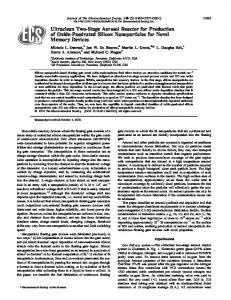
Preparation of Thin Dielectric Film for Nonvolatile Memory by Thermal Oxidation of Si-Rich LPCVD Nitride Hei Wong, M. C. Poon, Yong Gao and Ted C. W. Kok J. Electrochem. Soc. 2001, Volume 148, Issue 5, Pages G275-G278. doi: 10.1149/1.1362552 Email alerting service
Receive free email alerts when new articles cite this article - sign up in the box at the top right corner of the article or click here
To subscribe to Journal of The Electrochemical Society go to: http://jes.ecsdl.org/subscriptions
© 2001 ECS - The Electrochemical Society
Journal of The Electrochemical Society, 148 共5兲 G275-G278 共2001兲
G275
0013-4651/2001/148共5兲/G275/4/$7.00 © The Electrochemical Society, Inc.
Preparation of Thin Dielectric Film for Nonvolatile Memory by Thermal Oxidation of Si-Rich LPCVD Nitride Hei Wong,a M. C. Poon,b Yong Gao,b and Ted C. W. Kokb a
Department of Electronic Engineering, City University, Kowloon, Hong Kong Department of Electrical and Electronic Engineering, The Hong Kong University of Science and Technology, Kowloon, Hong Kong
b
In this work, we develop methods for fabricating high quality dielectric films for nonvolatile memory applications. Oxide/Si-rich nitride/oxide structures are fabricated where the Si-rich nitride layer was deposited by the low pressure chemical vapor deposition 共LPCVD兲 technique. With a Si-rich nitride layer, the Fowler-Nordheim tunneling voltage can be cut down to 3 V for oxide thickness of about 100 Å. By reoxidizing the Si-rich nitride layer, secondary ion mass spectroscopy study reveals that the hydrogen content of nitride film and its interface can be reduced by more than 40%. With this method, high nitrogen content oxynitride and smoother oxynitride/oxide interfaces result and the interface charge trapping can be improved remarkably. © 2001 The Electrochemical Society. 关DOI: 10.1149/1.1362552兴 All rights reserved. Manuscript submitted September 13, 2000; revised manuscript received January 22, 2001.
Flash memory has now become an important portion of the semiconductor memory market due to the wide application of embedded microprocessor system. The storage density will be increased further and the fabrication technology is driven even closer to its technological constraints. New reliability challenges are present because of the increasing memory size and the down scaling device size.1-5 Tunnel oxide reliability is one of the most crucial concerns. As other nonvolatile memory families, the retention time requirement for flash memory is generally over 10 years.5 This requirement calls for a very low leakage tunnel oxide. However, in a very thin oxide, the interface region is so large 共when compared to the total oxide thickness兲 that the interface traps can play a dominant role in the tunneling characteristics. On the other hand, the number of electrons stored in the floating gate will be scaled to about 3000 in the 1 Gbit generation,5 thus any mobile ion contamination will cause significant charge fluctuation. According to the current approach, the maximum acceptable concentration of mobile ions in the new generation memory cell will be less than 0.3 parts per billion 共ppb兲.5 All these critical reliability issues are related to the gate dielectric preparation. Oxide-nitride-oxide 共ONO兲 structure was considered as a good structure and has been used as dielectric in electrically erasable programmable read only memory 共EEPROM兲 devices.6-7 In comparison to thermal oxide, the ONO structure has lower leakage current, higher effective dielectric permittivity, and higher reliability.8-11 However, these characteristics are still not good enough for the crucial constraints of 1 Gbit flash memory application. Silicon nitride, prepared by chemical vapor deposition 共CVD兲 and because of the inherent stain in the networks of the amorphous structure, is not in good device quality.12 Oxynitride by NH3 nitridation would introduce a large amount of traps because of the hydrogen incorporation.13-15 Although N2O nitridation seems to have the advantage of low hydrogen content, the amount of nitrogen incorporation, in the range of 2-4 atom %, is still not large enough to improve the hardness for hot carrier irradiation.16 This work aims to study the properties of silicon-rich silicon nitride and oxynitride prepared by oxidation of silicon-rich silicon nitride. Secondary ion mass spectroscopy 共SIMS兲 was used to study the physical structure and chemical compositions. Current-voltage 共I-V兲 and capacitance-voltage 共C-V兲 measurements were conducted to study the charge transport mechanism and the dielectric trap properties of these materials. Experimental Sample preparation and measurement.—Samples with oxide/ oxynitride/oxide structure were fabricated on n-type silicon with 具100典 orientation and the resistivity is in the range of 4-10 ⍀ cm. A thin thermal oxide of about 100 Å was first grown with dry oxidation at 850°C, and then a thin 共⬃130 Å兲 silicon nitride or
silicon-rich nitride layer was deposited on the thermal oxide using low pressure chemical vapor deposition 共LPCVD兲 at 820°C. The chemical sources used for the LPCVD are SiCl4 and NH3. Details of the process parameters for different samples are listed in Table I. Some of the samples were than reoxidized at 1000°C for 35 min to form ONO structure. For SIMS depth profiling, a Riber MIQ256 SIMS instrument was used. The beam source is 1 keV Cs⫹ and the beam current is 50 nA. The negative secondary ions were selected with a quadrupole filter. The room temperature I-V characteristics and C-V characteristics are measured with Keithley 236 source measurement tools and a 590 CV system, respectively. Results and Discussion SIMS measurements.—Figure 1 depicts the SIMS depth profile of various samples. As shown in the figure, remarkable oxygen and nitrogen tails are found due to the ion recoil as a result of 1 keV Cs⫹ ion sputtering. Although the SIMS spectra may not reflect the real distribution of atoms and bonds in these samples,6,17 it still provides useful information for the comparative study concern. The bulk nitrogen concentration is as high as 70 atom % 共sample B兲. With reoxidation, the top oxide layer is about 50 Å and the nitride layer is about 130 Å 共sample E兲. For the silicon-rich sample 共sample C and its reoxidized one, sample F兲, the bulk nitrogen concentration is significantly lowered to less than 45 atom % as a result of introducing excess silicon atoms. The excess silicon will have significant effects on the current conduction of the dielectric films and will participate actively in future oxidation process. The physical configurations of the atoms in network are confined by the bending and stretching forces. It was found that these constraint forces are a linear function of the average coordination number of the atoms.12 For SiO2, the average coordination number is 2.67 and is optimal because bending forces at oxygen atoms are too weak to function as significant constraints. In silicon nitride the corresponding coordination number is 3.43 and the networks are overconstrained. As the silicon atom stretching constraints are stronger than bending constraints, strain energy will be accumulated along the bending constraints in silicon nitride. The average bond angle is distorted and more defects result. The difference in the
Table I. Process parameters and thin film properties. Sample
A
B
C
D
Bottom oxide 100 100 100 100 CVD nitride — 129 128 128 Si/N ratio — 0.75 0.85 0.90 Top oxide — — — —
E 共ONO兲 F 共ONO兲 G 共ONO兲 100 127 0.75 40
100 124 0.85 40
100 124 0.90 40
G276
Journal of The Electrochemical Society, 148 共5兲 G275-G278 共2001兲
Figure 2. SIMS hydrogen profile for various samples.
tween 5.9 eV 共nitride兲 and 8.9 eV 共oxide兲. The grade interface is more effective in reducing direct tunneling and interface defect density. Figure 2 displays the hydrogen profiles of various multilayer dielectrics. It is found that a large number of hydrogen impurities are introduced by the LPCVD process. The hydrogen concentration was defined as a ratio of the secondary ions with mass 29 共SiH⫺兲 to ions with mass 30 共NO⫺兲. The hydrogen concentration is the highest near the surface. It decreases gradually and then increases slightly at the interface. Stoichiometric silicon nitride 共sample B兲 has the highest hydrogen content. Silicon-rich samples have a lower amount of hydrogen. For Si-rich samples with reoxidation 共sample F兲, the
Figure 1. 共a兲 SIMS nitrogen profiles for various Si-rich nitride films. Nitrogen and oxygen depth profiles for ONO structure prepared by reoxidation of 共b兲 stoichiometric silicon nitride; and 共c兲 Si-rich silicon nitride.
bending constraints also results in the poor Si/Si3N4 interface. Oxynitride is a good approach for improving the dielectric properties. It can be used for bridging the oxide and nitride and their interface to silicon substrate. The nonstoichiometric silicon oxynitride 共with excess silicon兲 may consist of Si-O, Si-N, and Si-Si bonds. To the first order approximation, its bandgap is expected to vary linearly be-
Figure 3. I-V characteristics of the multilayer dielectric films.
Journal of The Electrochemical Society, 148 共5兲 G275-G278 共2001兲
G277
Figure 4. Band diagram of Si-rich nitride/oxide structure illustrating the tunneling current enhanced by excess silicon.
hydrogen content decreases by more than 40% and there is no noticeable hydrogen peak at the interface. Hydrogen was found to be traps centers under hot electron irradiation.18,19 According to Hori et al.,19 electron injection induced flatband shift (⌬V FB) of NH3 nitrided oxide can be approximated by ⌬V FB ⫽ K 关 H 兴
关1兴
where K is a constant of about 9.3 ⫻ 10⫺22 V cm3 and 关H兴 is the hydrogen concentration in the oxynitride. Thus the proposed method is an effective measure to reduce the electronic trapping. Our C-V measurement results 共see the section on C-V measurement兲 also agree with this relationship. In Si-rich samples, the excess silicon atoms should exist in the form of wSi-H, which can be broken under hot electron or high field stressing and become an electron trap.18,19 With reoxidation, oxynitride is formed and the hydrogen concentration can be removed significantly. Si-rich SiOx Ny consists of Si-O, Si-N, and Si-Si bonds and the chemical reactions for the oxidation of siliconrich nitride could be very complicated. However, the key reactions should involve the following process 2 wSi-H ⫹ O2 → wSi-O-Siw ⫹ H2
关2兴
2wSi2NH ⫹ 2wSiH ⫹ O2 → 2wSi3N ⫹ H2O
关3兴
2 wSiNH2 ⫹ wSi-H ⫹ O2 → wSiOH ⫹ wSi2NH ⫹ H2O wSiOH ⫹ wSiH⫹ → wSi-Siw ⫹ H2O
关4兴 关5兴
Reactions 2-5 describe, on the atomic scale, the possible reactions take place during the silicon nitride oxidation in terms of chemical bonds rearrangement. These reactions involve in the elimination of hydrogen-containing species and results in the removal of potential trap centers.
Figure 5. C-V characteristics of the samples.
I-V measurement.—In the present flash structure, the floating gate is isolated completely by oxide. To program or to erase the memory content involves applying a very large field to the devices and causes reliability problems in long-term operation. In next generation flash memory, we require an extremely reliable dielectric with respect to high field stressing. To extract the charges from the floating gate with a reasonable low voltage in the scaled structure, a thin dielectric of about 100 Å or less is required. These two constraints cannot be satisfied at the same time with the available technology. Figure 3 shows the I-V characteristics of several different dielectric films. The Fowler-Nordheim 共FN兲 threshold voltage is about 8 V for oxide thickness of 100 Å. By covering the same oxide with a silicon-rich nitride layer about 130 Å thick, the threshold voltage was reduced to about 3 V with a relative thick dielectric film. This characteristic is particularly useful to low voltage flash memory application. The phenomenon can be explained as follows. The excess silicon atoms in the dielectric film act as trap centers which assist the electrons to transport in the Si-rich nitride layer.20 Figure 4 shows the band diagram of the structure under accumulation. The Si-rich nitride layer has a lower bandgap, and it results in an energy difference between the Si-rich nitride and oxide. This energy difference provides an excess energy which results in the acceleration of electrons toward the interface. This structure in effect reduces both the height and depth of the barrier at the oxide/silicon interface and enhances the FN tunneling. Note that the enhancement of current could only be found in the structure with Si-rich nitride layer. In addition, since reverse biasing does not give rise to tunneling current enhancement, the longer retention time can be maintained in practical low voltage flash application. These behaviors were not observed
Table II. Flatband shift and fixed oxide charge of some typical samples. Sample Si/N ratio Flatband (V) C sc (F) Fixed charge Density 共cm⫺2兲
A
B
C
E 共ONO兲
F 共ONO兲
— ⫺0.8 2.3 ⫻ 10⫺11 9.20 ⫻ 1010
0.75 ⫺2.1 2.44 ⫻ 10⫺11 3.39 ⫻ 1012
0.85 ⫺2.1 2.45 ⫻ 10⫺11 3.54 ⫻ 1012
0.75 0.18 1.94 ⫻ 10⫺11 ⫺2.18 ⫻ 1011
0.85 0.7 1.95 ⫻ 10⫺11 ⫺1.14 ⫻ 1012
G278
Journal of The Electrochemical Society, 148 共5兲 G275-G278 共2001兲
in conventional stacked silicon oxide/nitride structure. With reoxidation, a multilayer 共oxide/oxynitride/oxide兲 structure was formed. SIMS profiling reveals that the surface layer is an oxide layer with thickness in the range of 50 to 80 Å depending on whether the silicon concentration of the as-deposited Si-rich nitride and the center layer is oxynitride. As mentioned earlier, due to its preparation technique and the large coordination number, the quality of LPCVD silicon nitride is poor and the even worse interface to oxide and silicon and hardly make it to be used in the active device structure. By introducing excess silicon and with reoxidation, a very good oxynitride can be achieved. The merits of post-CVD oxidation are threefold. First, it rehears the structural defects in the CVD nitride; second, it grades the oxide/CVD nitride interface by making the oxygen and nitrogen profiles smoother and releases the interface stress and the tunneling current can also be reduced; third, it removes the hydrogen atoms which will be trap centers for dielectric film under hot carrier irradiation. Note that these merits can only be achieved effectively with the introduction of excess silicon. As shown in Fig. 3, the breakdown voltage was increased to about 18 and 20 V for samples D and E, respectively. This technique is particularly useful in preparing a high quality smooth transition multilayer dielectric film. When compared to the oxynitride prepared by N2O annealing, it has the advantage of high nitrogen content which leads to a greater hardness for hot carrier irradiation. Since the hot carrier irradiation mainly occurs at the interface, instead of depositing Si-rich nitride on a thin silicon oxide layer, it may deposit on Si directly to maximize the hot carrier hardness in some applications. C-V measurement.—Figure 5 shows the high frequency 共100 kHz兲 C-V characteristics of various samples. Table II listed the flatband voltage and fixed oxide charge density calculated from the C-V curves. Pronounced negative shifts of flatband are found for samples with CVD nitride with excess silicon 共samples B and C兲 and positive shifts with reoxidation. It is noted that the 100 kHz C-V characteristics of the capacitor are similar to low frequency characteristics because of the presence of oxide charge. Instead of saturating at large forward bias, the large amount of oxide charge in gate oxide can invert the surface and the capacitance rises to C ox as the gate voltage swept to the strong inversion range. As shown in Table I, by covering the oxide layer with nitride, the fixed oxide charge density was increased by more than one order of magnitude. The charges could come from several sources including the inherent trap center of CVD nitride, the mismatch, and strain at the nitride/oxide interface. In addition, the excess silicon atoms also serve as both electron and hole traps.21-23 After reoxidation, a positive shift of flatband was found. It indicates the removal of negative charges. This shift could be due to the removal of structural defects in the CVD nitride and the less strained oxide/CVD nitride interface after reoxidation. Note that the effects of the hydrogen removal observed in SIMS measurement should not be reflected in this measurement for electrical characteristics, because the hydrogen bonds do not serve as trap centers under these measurement conditions. However, hydrogen bonds can be easily broken and become trap centers under high field stressing or hot carrier irradiation18,19 and cause reliability deg-
radation for long term operation of the devices. The significant removal of hydrogen content using the reoxidation of Si-rich nitride technique will improve the device reliability greatly and this work is still under investigation. Conclusions Oxide/Si-rich nitride/oxide structures have been fabricated and their properties have been studied in detail. With an LPCVD Si-rich nitride layer, the Fowler-Nordheim tunneling voltage can be cut down to 3 V for oxide thickness of about 100 Å. This multilayer dielectric structure can be used in low voltage flash memory. By reoxidizing the Si-rich nitride layer, secondary ion mass spectroscopy 共SIMS兲 study reveals that the hydrogen content of nitride film and its interface can be reduced by more than 40%. This lowhydrogen content oxide/oxynitride/oxide dielectric film can be used in high reliability nonvolatile memory. Compared to oxynitride prepared by other techniques, this method results in a high nitrogen content oxynitride film and smoother oxynitride/oxide interfaces and the interface charge trapping can be improved remarkably. However, it should be noted that the thickness and quality of the tunneling oxide layer is still the ultimate constraint for using this fabrication technology for flash applications. Acknowledgment The authors would like to thank Dr. A. M. Myasnikov for making SIMS measurements. This work was partially supported by research project no. 7001134 of City University. References 1. E. Takeda, Microelectron. Reliab., 37, 985 共1997兲. 2. P. Cappelletti, Microelectron. Reliab., 38, 185 共1998兲. 3. S. Atitome, R. Shirota, G. Hemink, T. Endoh, and F. Masuoka, Proc. IEEE, 81, 776 共1993兲. 4. Y. B. Park and D. K. Schroder, IEEE Trans. Electron Devices, 45, 1361 共1998兲. 5. A. Modelli, Microelectron. Eng., 48, 403 共1999兲. 6. P. C. Fazan, A. Ditali, C. H. Dennison, H. E. Rhodes, H. C. Chan, and Y. C. Liu, J. Electrochem. Soc., 138, 2052 共1991兲. 7. S. Minami and Y. Kamigaki, IEEE Trans. Electron Devices, 40, 2011 共1993兲. 8. V. A. Gritsenko, H. Wong, J. B. Xu, R. M. Kwok, I. P. Petrenko, B. A. Zaitsev, Yu. N. Morokov, and Yu. N. Novikov, J. Appl. Phys., 86, 3234 共1999兲. 9. V. A. Gritsebko, Yu. G. Shavalgin, P. A. Pundur, H. Wong, and W. M. Lau, Microelectron Reliab., 39, 715 共1999兲. 10. V. A. Gritsenko, S. N. Svitasheva, I. P. Petrenko, H. Wong, J. B. Xu, and I. H. Wilson, J. Electrochem. Soc., 146, 780 共1999兲. 11. V. A. Gritsenko, I. P. Petrenko, S. N. Svitasheva, and H. Wong, Appl. Phys. Lett., 72, 462 共1998兲. 12. G. Lucovsky and J. C. Philips, Microelectron. Eng., 48, 291 共1999兲. 13. H. Wong and Y. C. Cheng, J. Appl. Phys., 74, 7364 共1993兲. 14. H. Wong, B. L. Yang, and Y. C. Cheng, Appl. Surf. Sci., 72, 49 共1993兲. 15. H. Wong and Y. C. Cheng, J. Appl. Phys., 67, 7132 共1990兲. 16. T. Hori, H. Iwasaki, and K. Tsuji, IEEE Trans. Electron Devices, ED-36, 340 共1989兲. 17. I. Banerjee and D. Kuzminov, Appl. Phys. Lett., 62, 1541 共1993兲. 18. H. Wong and Y. C. Cheng, J. Appl. Phys., 74, 7364 共1993兲. 19. T. Hori and H. Iwasaki, Appl. Phys. Lett., 52, 736 共1988兲. 20. H. Wong and Y. C. Cheng, J. Appl. Phys., 70, 1078 共1991兲. 21. V. A. Gritsenko, Y. N. Novikov, Y. N. Morokov, and H. Wong, Microelectron. Reliab., 38, 1457 共1998兲. 22. V. O. Sokolov and V. B. Sulimov, Phys. Status Solidi B, 135, 369 共1986兲. 23. J. K. Rudra and W. B. Fowler, Phys. Rev. B, 35, 8223 共1987兲.