Ching-Che Chung, Pao-Lung Chen, and Chen-Yi Lee. Dept. of Electronics Engineering / National Chiao Tung University. Hsinchu, Taiwan, R.O.C.. ABSTRACT.
An All-Digital Delay-Locked Loop for DDR SDRAM Controller Applications Ching-Che Chung, Pao-Lung Chen, and Chen-Yi Lee Dept. of Electronics Engineering / National Chiao Tung University Hsinchu, Taiwan, R.O.C. After DLL is lock, the total input clock period.
ABSTRACT This paper presents an all-digital Delay-Locked Loop (DLL) for DDR SDRAM controller applications. The presented all-digital, cellbased, DLL-based five-phase multi-phase clock generator can generate the required fixed timing delay (tSD) for DDR SDRAM controller to capture the output data (DQ) correctly. The proposed DLL-based multi-phase clock generator architecture can lock to the harmonic of input clock period and still get a correct multi-phase clock output. Hence the design challenges to build a high resolution delay line with minimum intrinsic delay can be reduced. Simulation results and chip measurement results show that the proposed DLL can generate desired tSD delay with error < 7.6%). The power consumption of the proposed DLL is 4.1mW (at DDR-200) and is 9.0mW (at DDR-400).
However, if the required numbers of output multi-phase signals areincreased or the required maximum operating frequency si increased, DLL architectures [3, 5] will face difficult design challenges to build a high resolution delay cell with minimum intrinsic delay requirement. As a result, the operating range of previous DLL is severely limited. In this paper, the new DLL-based multi-phase clock generator architecture is proposed to let the DLL lock to harmonic of the input clock period and can still get a correct multi-phase clock output. The proposed architecture can reduce the design challenges to build a high resolution delay line with minimum intrinsic delay. Hence the frequency operating range of DLL can be improved.
INTRODUCTION
tSD|
_
Delay-Locked Loops (DLLs) have been widely used for designing high-speed memory interface circuit or clock multiplier to perform clock de-skew [2, 4] and multi-phase clock generation [3, 5]. In those applications, the DLL offers better jitter performance than Phase-Locked Loop (PLL) because the reference clock jitter and the noise induced by power supply noise or substrate noise disappear at the end of the delay line. On the other hand, the ring oscillator of PLL accumulates jitter and noise effects. Thus DLL is good alternative for PLL in those applications and has a good phase tracking ability.
tSD
All DQ and DQS Setu
Total
Strobe
Budget Ujncertainty
In Double Data Rate (DDR) SDRAM controller design, the output data strobe (DQS) signal must be delayed by a fixed timing delay (tSD) to capture the output data (DQ) correctly. Figure 1 shows this read operation timing budget. Ideally, the DQS and DQ is edge aligned by DDR SDRAM. However due to pin-to-pin skew among all DQ and DQS, and PCB board skew, the data valid window becomes smaller than expected. As a result, how to generate an optimal timing delay (tSD) to make sure that both setup/hold time budget for the controller can be met, has become an important design issue for DDR SDRAM controller design.
Skew
Data Valid
Hold
Buge Skew
FIGURE 1. READ OPERATION TIMING BUDGET
The proposed DLL is implemented with a 0.13ptm 1P8M CMOS process Structured ASIC cell-library. Frequency operating range of the proposed DLL ranges from 100MHz to 200MHz to meet the DDR-200/266/333/400 specifications. The power consumption of the proposed DLL is 4.1mW (at DDR-200) and is 9.0mW (at DDR-400).
In [1], the calculations for timing budget show that the optimal value for tSD is approximately 20 percent of an input clock period. Since the input clock frequencies range from 100MHz to 200MHz (DDR-200/266/333/400), the tSD value varies from 2ns(=1OnsxO.2) to Ins (=5nsxO.2). In this paper, a five-phase, all-digital, cell-based, DLL-based multi-phase clock generator architecture is proposed to generate this desired tSD delay for DQS signal. The proposed design can overcome process, voltage, and temperature (PVT) variations
PROPOSED DLL ARCHITECUTRE The proposed DLL architecture is shown in Figure 2. Like most of DLL-based multi-phase clock generators [3,5], the DLL has a multi-stage delay line with the same control code (dline control) to generate equally spaced multi-phase clock output. The TDC, which used in the close-loop for reference clock (FREF) period measurement [5], provides the range selection control for the DLL controller.
and still generate the desired tSD delay.
DLL-based multi-phase clock generator must have anti-harmonic lock capability. Otherwise the multi-phase clock generation will be failed. In previous DLL design [3-4], the lock detector is used to overcome the possibility to lock to the harmonic of input clock period. A similar concept is proposed in [5], it uses a Time-to-Digital Converter (TDC) to perform period measurement to avoid false-lock,
1-4244-0180-1/06/$20.OO ©2006 IEEE
delay of whole delay line is the same as
In previous DLL designs [3-5], when DLL is locked, total delay of the whole delay line is equal to one period of the reference clock (TFREF). Hence each delay stage should have TFREF/5 delay. As a result, the design requirements for the minimum delay of each delay stage must be smaller than this delay value: TFREF/5 in the worst case.
1
Sometimes it is difficult to meet this minimum delay constraint when using standard cell to build up a high resolution delay cell. Thus in the proposed DLL, the TDC measures two periods of the reference clock period and makes the DLL lock to 2xTFREF. After DLL is locked, each delay stage should have 2xTFREF/5 delay. Hence the minimum delay constraint for each delay stage is extended twice as original. And the total delay from DQS to DQSD becomes 1.2XTFREF =3x (2XTFREF/5), which means the phase shift between DQS and DQSD is still 0.2xTFREF. As a result, the desired tSD delay can be generated by the proposed DLL. CKOUIT
Both range selection stage and coarse-tuning stage are implemented using path-selector [5] with different delay cells. The total controllable delay range of fine-tuning delay stage must cover the delay step size of coarse-tuning stage. For coarse-tuning stage, it also needs to cover the delay step size of range selection stage.
The maximum delay of one delay stage must be larger than
2XTFREF/5 in the best case (FF, 1.32V, -40°C), and minimum delay of
one delay stage must be smaller than 2xTFREF/5 in the worst case (SS,
1.08V, 125°C).
CKOUITC CKOUT2 CKOUIT4
CKOUIT3
Range
IN
Coarse Tuning
Selection
_
Fine
Tuning
OUT
P4i P
FRM
dline_control
Controller
_7
P. -
IF OUT
FChNoupreIfmlipaecoksrane.Totu
TDC --h--OLOutput delav line
IFCONIOI
n.iDQSD
Phase ks
Detector
F_IN
LOCK
D
FC0N1311I4
DQS
FIGURE 2. THE PROPOSED DLL ARCHITECTURE
FIGURE 3. THE PROPOSED HIGH RESOLUTION DELAY LINE
The output order of multi-phase clock is rearranged. The output multi-phase clock signals are also shown in Figure 2 and named as CKOUTO to CKOUT4. The phase shift between FREF and P2 is 0.2XTFREF= {3x (2TFREF/5) modulus TFREF}, thus it is rearranged as CKOUTO. Similarly, the phase shift of P0 is 0.4xTFREF, phase shift of P3 is 0.6xTFREF, phase shift of P1 is O.8xTF1REF, and phase shift of P4 is 0. As a result, the output multi-phase clock signals are mapped as follows: {CKOUT0, CKOUT1, CKOUT2, CKOUT3, CKOUT4}
The phase detector (PD) used in the proposed DLL is almost the same with the phase detector proposed in [6] but with some modifications for phase error detection ability enhancement. IN
FB QU QD QD OUTU OUTD
{P2,P0,P3,P1,P4}.
In the proposed DLL architecture, since DLL can lock to harmonic of input clock period and can still get a correct multi-phase clock output. The proposed architecture actually helps to improve multi-phase clock rate and helps to increase the numbers of multiphase clock signals with a high-speed reference clock input. On the other hand, it also increases the maximum operating frequency of the DLL.
QU
l
H
PLilse widtih extended OUTU
QDNPhase error inserted
CIRCUIT IMPLEMENTATION Figure 3 shows the circuit of one delay stage. The total delay line consists of five equal delay stages. The proposed delay stage is controlled by three cascading stage: range selection stage, coarsetuning stage, and fine-tuning stage.
QD QU
PLulse width extended
OUTD ---Phase error inserted
In fine-tuning stage, the digital-controlled varactor (DCV) [7] is T. . 4 IGRPH4ASE- DEPTPTn_cToRDA r 7ZONE MPT\IT7MIATTION areFIUE4PHSDTCOREAZNEMIIAIN used to achieve very fine resolution and those DCVs *~~~~~~~~~~~~~~~~~~~~~F( implemented with standard cells. In Figure 3, the change of fineFigure 4 shows modified circuit and signal waveforms for the tuning control code (FCON[3 1:0]) will finely adjust the capacitive loading on F_OUT net. The worst phase resolution of this fine-tuning proposed PD. In the proposed PD [6], phase detector only detects the stage is 1.4PS with good linearity when it is implemented with a sign of phase error (i.e. lead or lag). Both QU and QD are three-state 0.13pim 1P8M CMOS process Structured ASIC cell-library, and the PD's outputs to decide whether IN leads or lags FB. By using the digital pulse amplifier concept in [6] to extend the pulse width of QU total controllable delay range of this fine-tuning stage is 37ps. and inserting a delay on QD net, the generated OUTU pulse width can be further extended. It means the detected phase error is enlarged
2
by this improvement circuit. As a result, the minimum detectable phase error of this PD can be improved. Similarly, the modified circuit for OUTD pulse generation is also shown in Figure 4.
TDC and is converted into delay line range control code (range_control[2:0]) and then the delay line executes range selection.
After delay line finishes range selection, the total delay of the whole delay line falls into this range: 1.5 x TFREF < Tdelay- line < 2.0 x TFREF. Then the DLL controller continues fine-tuning the output phase accuracy with PD's UP/DOWN signal. Since the delay range of the delay line is determined first, thus the false-locked problem will not occur in the proposed design.
Thus the next stage digital pulse amplifier can more easily extend the OUT/OUTD pulse width to meet the output register's timing requirements. By carefully design the digital pulse amplifier to extend the three-state PD output pulse width, the dead zone of this PD can be reduced to 5ps when it is implemented with 0.13ptm 1P8M CMOS process Structured ASIC cell-library.
When the phase error between reference clock (FREF) and delay line output (P4 or CKOUT [4]) is smaller than PD's dead zone, the DLL is locked. Both multi-phase clock generation and tSD delay generation are completed.
Since the delay line output signal (P4) shown in Figure 2 has more capacitive loadings than the other multi-phase clock signals. Dummy cells must be added to the rest of multi-phase clock signals (PO-P3) to balance the loadings of each multi-phase clock signal. And during DLL placement and routing process, the delay stage must be placed and routed firstly, and then one delay stage layout is duplicated and is connected to build up the whole delay line.
l
_
TDC
DLL RESET
l _
DelayLineDL & Fine-Tuning
FIGURE 6. TRANSIENT RESPONSE OF THE DLL (AT DDR-200)
in *~~~~
~
t f; 4 ~~~~~~~~~~~~~~ Aa
_
2
_
_
0 0 ~~~~~~~~~~~~~~~~~~~~~~~~~~~~~~~~~eot
[03]E
FIGURE 5. LAYOUT OF THE PROPOSED DLL TEST CHIP
The total gate count of the proposed DLL is 5250, and the area of the proposed DLL is 452tm x 462pm. Figure 5 shows the layout of DLL test chip. A digital-controlled oscillator (DCO) is added on this test chip to use as the reference clock for DLL. And DLL can also take external clock as reference clock.
6l
0
Multi-Phase
Clock Signals
The proposed design can use normal auto placement and routing (APR) tools to generate the final layout with carefully writing timing constraints for each delay cell. Thus the proposed design actually reduces the design time and design complexity to build up the DLL
0-21 1[.
FIGURE 7. DLL AT STEADY STATE (AT DDR-400)
Figure 7 shows the proposed DLL at steady state. When DLL is locked, the generated multi-phase clock signals (CKOUT [4:0]) reach equal space in one reference clock period. And the phase shift between DQS and DQSD is O.2xTF1RJF. In this simulation, the DQS is
and ultiphae clck enertor
SIMULATION AND MEASURED RESULTS
assigned to reference clock, thus the phase shift between CKOUT [0]
and DQSD should be 0. (i.e.
Figure 6 shows the transient response of DLL after system reset. After system reset (i.e. PDN=1), the TDC performs reference clock (FREF) period measurement. The dline_in signal shown in Figure 6 becomes "low" for two reference clock periods. This pulse is sent to
tSD=O.2xTFREF).
The DLL continues to update the delay line control code and keeps tracking to the rising edge of reference clock. Since in the proposed DLL, only rising edge information of reference clock is used hence it also has good duty-cycle error immunity. Compared to
3
previous DLL [4], the extra duty-cycle correction (DCC) circuit is eliminated.
CONCLUSION In this paper, an all-digital delay-locked loop for DDR SDRAM controller applications is presented. The proposed DLL architecture
Post-layout Fast-SPICE simulations are performed in different operation conditions to make sure the stability of the proposed DLL. Table 1 lists the simulated tSD value vs. desired tSD value In different input conditions (DDR-200/266/333/400) and different operation environment, the generated delay error (AtSD) can still keep smaller than 7.600 of the desired tSD value, which meets the required delay error (< 130%o) as mentioned in [1].
can not only reduce design challenges to build up a high resolution
delay cell with minimum delay constraint, but also make it possible to implement with standard cells. Thus the proposed architecture can
reduce both design time and circuit complexity. And it is very
suitable for many high-speed interface circuit or digital communication applications.
ACKNOWLEDGMENT
TABLE 1. DLL IN DIFFERENT OPERATING CONDITION
Input
Desired tSD (ns)
DDR-200
2.0 1.5 1.2 1.0
DDR-266
DDR-333 DDR-400
1.08V, 125 OC 1.911 1.537 1.136 0.981
The author would like to thank their colleagues within the S12 group of National Chiao Tung University for many fruitful discussions. The Structured ASIC cell-library support from Faraday Technology Corporation is acknowledged as well.
Simulated tSD (ns) 1.2V, 1.32V, 25 °C -40°C 1.972 1.568 1.291 0.976
1.898 1.588 1.266 0.947
REFERENCES [1]
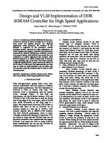
Figure 8 shows the measured DLL output waveform after DLL
lock*with The signal temperature. The lock with 1.2V 1 .2V power supply supply at room temperature. signal shown shown in channel 2 is reference clock (FREF), and the signal shown in channel 1 is CKOUTO. The reference clock is a 100MHz noisy clock source with rms jitter 269ps and PK-PK jitter 950ps. The jitter
[2]
atroom
11-Octt-05
lit 8 L ~~~~~~J* X Bt'JCJi 0I1J ns V i_ _50 _ _ Hpkpk( n
rs
_- L-1-
req(20
phase(12)
rms(B) BWL DC DC 6
3 trig onl 4 trig only
REDEFINE D MULTI ZOOM
10042:Ma Z 91lo233 104940 73-6E 69-3 89 2 0 0-95 ns 0.92 ns
pkpk(B) 1
RDEIN REDEFINE C
sCROLL PUTOISCIIROII
AUT
267 ps
pkpk(R)
1
.-_= _ --
;
__
in- 20100i
10 ns U 50 mV 2 5S mV
2001.
Eunseok Song, Seung-Wook Lee, Jeong-Woo Lee, Joonbae Park, SooIk Chae, "A Reset-Free Anti-Harmonic Delay-Locked Loop Using a Cycle Period Detector," IEEE J. Solid-State Circuits, Vol.39, pp. 2055,j 2061, Nov. 2004 [5] Ching-Che Chung and Chen-Yi Lee, "A New DLL-Based Approach for All-Digital Multiphase Clock Generation," IEEE J. Solid-State Circuits, Vol.39, pp. 469-475, Mar. 2004. Chung and Chen-Yi Lee, "An All-Digital Phase-Locked =[6]pp(R)Ching-Che Loop for High-Speed Clock Generation," IEEE J. Solid-State Circuits, 4 Vol.38, pp. 347-351, Feb. 2003. [7] Pao-Lung Chen, Ching-Che Chung, and Chen-Yi Lee, "A Novel Digitally-Controlled Varactor for Portable Delay Cell Design," IEICE Tran. Fundamentals, Vol. E87-A, pp. 3324-3326, Dec. 2004.
REDEFINE X 1 1410 1 X 1 < X 0; C[4] A1+=Jcy-cy (2) ti | Xt tB 8 < < Xt REDEFINE
+I,
0,50 V
fJ
GHz Clock Synthesizer and Temperature-Compensated Tunable Oscillator," IEEE J. Solid-State Circuits, Vol.36, pp. 417-423, Mar.
ZOOM * MATH
2
DC 166
40 0-12 0.13
;V
490
1089
1.56
237 2-8
127 057
I S
For MIath use
max
Chom, and Beomsup Kim, "A Low-Jitter Mixed-Mode DLL for High-
Speed DRAM Applications," IEEE J. Solid-State Circuits, Vol.35, pp. 1430-1436, Oct. 2000. [3] D.J. Foley, and M. P. Flynn, "CMOS DLL-Based 2-V 3.2-ps Jitter 1-
histogram of reference clock is also shown in Figure 8. 15:21:16
MICRON Technology Inc., "DDR SDRAM Functionality and Controller Read Data Capture", DesignLine, Vol.8, Issue 3, Sep. 1999. Jae Joon Kim, Sang-Bo Lee, Tae-Sung Jung, Chang-Hyun Kim, Soo-In
points
048| 25000000
4 GS/s
AUTO
FIGURE 8. MEASURE DLL OUTPUT (AT DDR-200)
Ideally, the phase shift between FREF and CKOUTO should be 360° + 5 = 72°, but due to the delay line resolution limitations, phase detector dead zone, and reference clock jitter effects, the measured phase shift between FREF and CKOUTO is 73.6°, which means the delay error is 44.4ps = (73.6°-72°).360°x10ns (at DDR-200). The jitter of output multi-phase clock signal CKOUTO is rms jitter 267ps and PK-PK jitter 920ps. The measured results show that the jitter performance of DLL output multi-phase clock signals is dependent on the reference clock jitter. But even with noisy reference clock input, the proposed DLL can still achieve lock and generate the required tSD delay. The power consumption of the proposed DLL is 4.1mW (at
DDR-200) and is 9.0mW (at DDR-400).
4