Microelectronics Reliability 65 (2016) 184–191
Contents lists available at ScienceDirect
Microelectronics Reliability journal homepage: www.elsevier.com/locate/microrel
Ball-grid-array solder joint model for assembly-level impact reliability prediction Chee Kuang Kok a,⁎, Wen Jie Ng a, Chin Chin Ooi b, Kia Wai Liew a a b
Faculty of Engineering and Technology, Multimedia University, 75450 Bukit Beruang, Melaka, Malaysia Motorola Solutions (M) Sdn. Bhd., 11900 Bayan Lepas, Penang, Malaysia
a r t i c l e
i n f o
Article history: Received 12 May 2016 Received in revised form 13 July 2016 Accepted 1 August 2016 Available online 9 August 2016 Keywords: Ball grid array Lead-free solder Dynamic impact Solder joint failure Finite element method
a b s t r a c t It has been well established that lead-free solder underperforms conventional leaded solder in reliability under dynamic impact. Common failures observed on ball-grid-array (BGA) solder balls on chip under board level impact include bulk solder ductile failure, intermetallic (IMC) layer crack and pad-lift. In this work, a finite element modeling approach was proposed to model bulk solder ductile failure and intermetallic layer crack. The use of beam elements and connector elements to represent the bulk solders and board/component side intermetallic layers, respectively, offers the advantage of simplicity over the use of continuum elements and cohesive elements for solder joints. This approach enables the modeling of assembly level impact with significantly less computational resources. The model was verified by comparing its prediction of BGA solder reliability against actual test results in a dynamic four-point bend test. The physical tests consist of ball impact at varying heights on a board with a mounted chip, and the subsequent analysis of the failure modes of the BGA solder joints. Simulation results were in good agreement with test results. The study shows that it is feasible to model BGA solder joint ductile failure and intermetallic layer crack under impact with simple elements with reasonable accuracy. © 2016 Elsevier Ltd. All rights reserved.
1. Introduction Portable device miniaturization and green-product requirement have led to the use of lead-free ball-grid-array (BGA) to connect chip package and printed circuit board (PCB). However, lead-free BGA is susceptible to drop impact failures [1]. Conventional solder bump shear and pull tests, usually performed at high (N 300 s−1) or low speed levels (b0.1 s− 1), fail to replicate BGA brittle interface failures at medium strain rate during dynamic impact [2]. In addition, it was found that BGA joint reliability correlated well with the percentage occurrence of interface bond failures and not solder interface fracture strength [3]. To characterize the BGA impact reliability, a number of experimental approaches had been proposed. Among them are JEDEC shock tower test [4], dynamic four-point bend test [5], dynamic spherical bend test [6], steel-rod-drop impact test [7], and Miniature Charpy Test [8]. These tests and other high-speed ball pull/shear tests are effective in unearthing common failures observed on ball-grid-array (BGA) solder balls under chip, including bulk solder ductile failure, intermetallic (IMC) layer crack and pad-lifts [9]. However, the availability of a model to reliably and accurately predict such failures will greatly save cost and time. There have been some successes in modeling BGA failures using the finite element method. Caroll et al. [10] proposed the use of connector elements to model individual solder joints in a BGA, and correlated ⁎ Corresponding author. Tel.: +606-2523648; fax: +60 6 2316552. E-mail address:
[email protected] (C.K. Kok).
http://dx.doi.org/10.1016/j.microrel.2016.08.001 0026-2714/© 2016 Elsevier Ltd. All rights reserved.
their model with experimental findings. Their model, however, did not distinguish bulk solder failure and IMC layer crack. Lall et al. [11] proposed the use of smeared property to model the solder interface, and compared it against another model using Timoshenko beam for individual solder. Their focus was to verify the use of sub-modeling approach for assembly level impact. Progressive damage of the joints was not modeled, which could limit the model prediction related to the solder joint progressive failures. In another effort, the use of cohesive elements for the solder interface was proposed [12], coupled with the sub-modeling approach [13]. However, it was not clear how the effect of sub-model changes, such as solder joint progressive failures, on the global model was accounted. Yeh and Lai [14], and Kim et al. [15] modeled one individual solder ball with many continuum elements, whose approach require significantly more computational resources than practically available for assembly level modeling. The primary challenge in finite element modeling of BGA failures for assembly level impact lies in the selection of elements for their available failure models and practicality, namely the accuracy and ease of modeling with reasonable amount of resources. The selection of failure models, in turn, depends on the availability of test data. While bulk solder material property can be obtained with standard and non-standard test methods, the efforts to quantify the tensile and shear strengths of IMC are relatively more involved. Past researchers had derived IMC failure data from characterization tests such as solder ball high-speed shear [15,16] and pull test [3,9,16], and compression test with micro-force tester [17] to isolate tensile and shear contribution to individual solder
C.K. Kok et al. / Microelectronics Reliability 65 (2016) 184–191
intermetallic bond failures. As a result of past efforts, there is now evidence that with increased strain rate, the failure mode of lead-free BGA shifts from ductile bulk failure and to brittle IMC interface failure [3,8,16]. In addition, the tensile/shear stress and strain at IMC interface failure is dependent on the strain rate, solder alloy, solder geometry, mask design, pad finishes and thermal history [18–20]. In this work, a dynamic four point-bend-test was conducted on a BGA package mounted on a test board. The dynamic four point-bendtest was chosen primarily due to its simplicity and cost effectiveness [21], and had been used by other researchers in similar efforts [6]. BGA failures were then analyzed and categorized into bulk solder failure, IMC failures and pad lift at board side and component side, respectively. A numerical model for use in assembly level was proposed to simulate BGA bulk solder and IMC failures to predict the BGA mechanical reliability under dynamic impact. The prediction agrees quite well with the experimental findings.
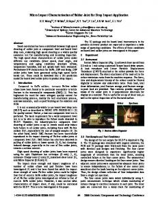
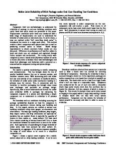
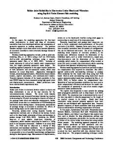
2. Experiment Fig. 1 illustrates the four-point dynamic impact test setup of the experiment. A steel ball of 136 g is dropped from varying heights as listed in Table 1. Each drop height was tested five times, each time on a fresh board with mounted chip. The corresponding initial velocity can be determined using the principle of conservation of energy. The ball impact upon the relatively stiff top span of 90 g (weight inclusive of bumper and rollers) then translates to deflection of the test board. The printed circuit board (PCB) dimensions are 75.0 × 40.0 × 1.08 mm. The BGA package is mounted at the bottom of the board, with its diagonals aligned with the sides of the board, such as shown in Fig. 2. A quarter of the PCB, such as shown in the dashed box, is use for modeling purposes. Table 2 gives important BGA solder ball properties, while Fig. 3 is a schematic of a solder ball and its surrounding geometry. Upon completion of the impact test, BGA failures were then analyzed using the red dye test [22,23] with the following procedure. Flux from the board and package was first removed by soaking the board with BGA package
185
Fig. 2. Bottom view showing the placement of the BGA package on PCB.
Table 2 Solder ball properties. Solder composition Solder ball diameter Pad type Pad pitch Pad finish Pad diameter Pad thickness
95.5Sn/3.8Ag/0.7Cu (SAC387) Nominal 0.40 mm Solder Mask Defined (SMD) 0.65 mm OSP 0.381 mm 0.135 mm
in flux removal solvent such as Ensolve for at least 1 h, with the help of ultrasonic agitation. After cleaning, the board was rinsed in water to remove the residual cleaner, and the board dried using compressed air. Red dye (i.e. Dykem Red Layout Fluid) was applied sufficiently underneath the package using a pipette, upon which the board was placed under vacuum (˜25 in. of Hg) for about 30 s to facilitate dye flow through solder joints. The board was then left in an oven at 100 °C for at least 30 min to dry the dye. Package was then removed by prying, and the dye-penetrated sites were failure sites ready for visual inspection using a stereo microscope. A joint with N80% of dye penetration was considered to have failed. Observed failures were then categorized into bulk solder failure, IMC failures and pad lift at board side and component side, respectively, such as illustrated in Fig. 4. 3. Simulation ABAQUS commercial finite element software was used to model the four-point dynamic impact test to simulate bulk solder ductile failure and IMC layer crack failure. Due to the symmetry of the board, the
Fig. 1. Four-point dynamic impact test setup.
Table 1 Ball drop height and initial velocity. Ball drop height (mm)
Velocity before impact (mm/ms)
166 254 361 488 636
1.805 2.232 2.661 3.094 3.532
Fig. 3. Solder ball and its surrounding geometry.
186
C.K. Kok et al. / Microelectronics Reliability 65 (2016) 184–191
Fig. 4. Different types of BGA failures. (a) Bulk solder failure; (b) IMC failure; (c) Pad lift.
Fig. 5. Quarter model of the four-point dynamic impact test.
BGA package as well as the rest of the test setup, only a quarter of the full model needs to be represented. The quarter model finite element mesh is depicted in Fig. 5. The impact ball and all the jig pieces were modeled using rigid elements, as they are significantly stiffer than the PCB and the mounted BGA package. A quarter of the weight of the ball and the top-span jig piece was used for the quarter model. The top span (roller to roller) is 35 mm while the bottom span is 60 mm. The PCB was modeled with eight layers of reduced integration brick elements (i.e. ABAQUS C3D8R), with an average in-plane mesh size of 0.85 mm. The mesh size was refined to around 0.15 mm at the BGA locations. The number of layers and in-plane element size were determined by performing a correlation study between experiment and simulation of static bending of the board. A layer of membrane elements was added to the exterior of the PCB for reporting of in-plane stress and strains. The BGA package was modeled with second ordered modified tetrahedron element (i.e.
ABAQUS C3D10M). The package is 13 mm × 13 mm × 0.885 mm (thickness excluding the BGA), with 19 × 19 solder joints in rectangular array. The bumper was modeled as a combination of a non-linear spring and a dashpot in parallel. The force-displacement curve of the bumper was determined via a static compression test to model the quartered nonlinear spring. The bumper damping coefficient cannot be determined with certainty, and has been assumed to be 100 Ns/m, quartered to 25 Ns/m. The effect of varying damping coefficient has been verified to be insignificant to the dynamic amplification of the PCB response. It is worth pointing out that the simulation did not capture the subsequent impacts of the steel ball after rebound. Although the ball rebounded in the physical test, the rebound has not been considered in the current FEA modeling. The impact upon rebound is assumed to be negligible due to small rebound height. Mechanical properties of various components were tabulated in Table 3, with their sources listed. In addition, bulk solder strain rate
Table 3 Material properties of major components.
Component
Young's modulus, E (MPa)
Poisson's ratio
Density, ρ (kg/m3)
SAC387 PCB⁎ Molding compound⁎ Copper pad IMC layer (Cu6Sn5)
41,730 25,000 16,000 [28] 120,000 86,000 [28]
0.35 0.16 0.3 0.34 0.25 [28]
7440 2340 1970 8900 8280
⁎ Unpublished data from vendors.
Failure criteria
Source
Mises plastic strain of 0.005 Nil Nil Nil 32 MPa (normal) 670 MPa (shear)
[24,26,27]
[25,29] [20]
C.K. Kok et al. / Microelectronics Reliability 65 (2016) 184–191
187
Fig. 6. BGA model. (a) Half and full beam elements (with connector elements at both ends of the beam invisible); (b) a BGA model with connector elements at beam's ends. Dash boxes highlight beam or connectors.
dependent elastic-plastic mechanical properties [24] were adopted in the solder beam elements. Copper pad plasticity was modeled using Johnson-Cook after ref. [25]. In this study, each solder ball was modeled using a first-order, threedimensional Timoshenko beam element (i.e. ABAQUS B31) of constant
circular cross-section with both ends being IMC layers represented by bushing connector elements (i.e. ABAQUS CONN3D2), having three translational and three rotational degree of freedom. Care was taken to ensure that the beam and connector elements on the planes of symmetry were halved, while the ones sharing two planes of symmetry
Table 4 BGA failure modes and failure sites.
Ba all Drrop Heeigh ht mm m) (m
Bestt Casee
E perimentt Exp Wor W rst Casse
Sim mulattion n
166
254
361
488
636
Board side IMC failure Component side IMCfailure
Board side pad lift C Component side pad lift
Bulk Solder Failure Combined Mode
188
C.K. Kok et al. / Microelectronics Reliability 65 (2016) 184–191
were quartered. Details are in Fig. 6. The modeling of the beam does not include SMD. The assumption of constant cross section of each beam had been justified by Lall et al. [11]. The IMC is assumed to have a constant thickness of 5 μm. The bulk solder is assumed to fail when its Mises plastic strain exceeds 0.005. On the other hand, the IMC layer is assumed to obey the following failure criterion, often used in modeling spot weld [30]:
f F¼ zþ Fn
qffiffiffiffiffiffiffiffiffiffiffiffiffiffiffiffiffiffiffiffi 2 2 fx þ fy Fs
ð1Þ
where fz is the connector axial force, and fx and fy are two perpendicular forces in the transverse directions. Fn is the IMC layer ultimate tensile force and Fs its ultimate shear force. The connector fails when the equivalent force, F, exceeds unity. The ultimate tensile and shear strengths were 32 MPa [31], and 670 MPa [20], respectively. At failure, the connector elements (i.e. IMC layer) will detach from their neighboring elements. A joint was assumed to have failed by the first failure mode it exhibited. When more than one failure mode occurred at a joint simultaneously, then the joint had a combined failure mode. The simulation was run for such duration that no further joint failure was observed. In this case, the duration ranged from 3 ms (lowest impact) to 9 ms (greatest impact). It is worth noting in many other studies [11,32,33], each solder ball was modeled with brick elements consisting of many nodes and elements. Failure criteria at the bulk solder may involve the use of Mises stress or strain, and that at the IMC the use of cohesive element with damage evolution. While this approach may better represent the behavior of a single solder joint, such approach may not be practical for modeling assembly level impact. A typical finite element model of any electronic device may easily consist of millions of elements, exclusive of the BGA joints. As such, the current approach of using one beam element and two connector elements to represent one solder joint is preferable, as it significantly saves
computational resources and decreases the computational time for each analysis. 4. Results and discussion A comparison of the experimental and simulated BGA failure modes and failure sites is tabulated in Table 4. Only a quarter of the BGA was presented in the table for comparison although the failures in the experiments were recorded in full. It is noted that in the actual experiment, such perfect symmetry was not obtained, although the failure sites exhibit a certain degree of symmetry. This imperfection may most likely be due to the slight offset of the ball impact location, an inevitable error associated to the ball being dropped at the impact site with the help of a tube with some clearance. Other sources of discrepancies include material and processing induced joint-to-joint variations. In the table, the combined mode refers to combined failures usually consisting of more than one failure type. The best case (least number of failures) and the worst case out of five test results for each drop height were reported. For comparison between simulation and experiment, any quarter of the BGA in the experiment was given equal weightage. The experimental best and worst cases can deviate significantly, as can be observed in Table 4. This scatters in experimental findings can be due to any of the aforementioned reasons, including variations in material, processing and test parameters. In this respect, simulation offers an advantage over the physical test, in which it gives precisely one failure result for each drop height. There is a reasonably good agreement between experiment and the simulation findings. The primary mode of failures in both the experiment and the simulation is board side IMC failures. The number of sites exhibiting this failure mode increases with increasing drop height. This is consistent with many experimental findings on the effect of dynamic loading on solder joint, namely high strain rate often leads to ductile (bulk solder)-to-brittle (IMC) failures [34]. In addition, these failures seem to concentrate at the chip corner along the board longer side (i.e. the right corner of the quarter BGA in Table 4). The latter was
Fig. 7. BGA joint failure propagation for ball impact height of 636 mm. (a) t = 0.38 ms; (b) t = 0.48 ms; (c) t = 0.62 ms; (d) t = 1.89 ms; (e) t = 3.48 ms; (f) t = 5.19 ms.
C.K. Kok et al. / Microelectronics Reliability 65 (2016) 184–191
expected, as the stretching and bending of ball joints will be the severest at the outer corner by analysis [1,35]. The stretching and bending are due to the fact that the package did not acquire the curvature of the bent board during the impact. In addition, the experimental results show significantly fewer failures at the chip corner along the shorter side (i.e. the bottom corner of the quarter BGA in Table 4). This is consistent with plate theory, in which a plate such as PCB will be more difficult to bend about its shorter side [36]. The simulation also predicted the same trend, albeit with more failures at the same corner than those observed in the experiment. It is clear from the test results that bulk solder failure was not a major concern (only observed in 6 joints out of 9025 joints in the entire 25 tests). This is also consistent with the simulation findings, in which the bulk solder failure was not the first failure mode of a failed joint in all cases. A few bulk solder failures were observed in simulation, but they all occurred only after connector failures (i.e. IMC layer crack) due to beam crushing, and therefore considered artefact. Table 4 clearly demonstrates the fact that BGA failures did not propagate in a linear fashion. In other words, failures did not simply occur at more locations at greater impact, while the failure types and locations for a less severe impact were preserved. This is evident in both the
189
experiment and the simulation results. At hindsight, it may be obvious that as one joint fails, there is a change in the overall constraint, affecting the mechanics of the neighboring elements. This could be an issue of concern for the use of sub-modeling approach, which assumes a global model relatively unaffected by the local changes. The propagation of different types of BGA failures in the simulation is essential in understanding the failure mechanics. While test results offer little insight on failure propagation, simulation provides useful visualization on how the BGA joint damage propagates. By plotting the failure types and sites at different time frames for the greatest drop height (Fig. 7), one can clearly see the types and locations of failures at different time frame. In this case, IMC failure starts at the outer corner as expected, and propagates inwards as time progresses. Significantly fewer failures were seen at the other corner. Failures also seem to cluster at certain time frames when the stress waves were the greatest. Fig. 8 provides visualization of the BGA joint failures between t = 0.300 ms to t = 1.875 ms for the case with the greatest impact. Notice how the PCB deflected as the time progressed, and how much more the deflection was relative to that of the package. The difference led to the IMC failures, upon which bulk solders detached from the component and/or the PCB. The detached bulk solder then flew off from their original locations.
Fig. 8. BGA joint failure from t = 0.300 ms to t = 1.875 ms. (a) t = 0.300 ms; (b) t = 0.375 ms; (c) t = 0.450 ms; (d) t = 0.600 ms; (e) t = 0.675 ms; (f) t = 0.975 ms; (g) t = 1.500 ms; (h) t = 1.875 ms.
190
C.K. Kok et al. / Microelectronics Reliability 65 (2016) 184–191
Fig. 9. In-plane maximum strain on PCB from t = 0.300 ms to t = 1.875 ms.
Fig. 9, depicting the in-plane maximum strain on the PCB, may further assist in the visualization of the failure propagation, when compared to Fig. 8. 5. Conclusion The following conclusions are made: (a) The use of beam elements and connector elements to represent bulk solder and the IMC layers, respectively, greatly simplifies the need to model each solder with multiple elements and the IMC layer with cohesive elements. (b) The proposed model, despite its simplicity, results in failure prediction that is consistent with experiment findings. (c) BGA failures do not propagate in a linear fashion. Failure of one joint will affect the mechanics of its surrounding. (d) Simulation offers a single prediction against the scatters in the experimental results, in addition to providing insights on failure propagation not usually available in the experiment.
Acknowledgment The authors would like to acknowledge the technical assistance of Motorola Solutions (M) Sdn. Bhd. Employees, Mr. Ong Choon Gim and Ms. Cheah Ui Ping, in providing the ground work for this effort. This research did not receive any specific grant from funding agencies in the public, commercial, or not-for-profit sectors. References [1] E.H. Wong, R. Rajoo, Y.W. Mai, S.K.W. Seah, K.T. Tsai, L.M. Yap, Drop Impact: Fundamentals & Impact Characterisation of Solder Joints, Electronic Components and Technology Conference 2005, pp. 1202–1209, http://dx.doi.org/10.1109/ECTC. 2005.1441423. [2] E.H. Wong, et al., Shear-strain characteristics of tin-based solder alloys at medium strain rate, Mater. Lett. 62 (2008) 3031–3034. [3] A.T. Valota, et al., High Speed Pull Test Characterization of BGA Solder Joints, 7th International Conference on Thermal, Mechanical and Multiphysics Simulation and Experiments in Micro-Electronics and Micro-Systems, EuroSimE 2006, pp. 1–6, http://dx.doi.org/10.1109/ESIME.2006.1644005. [4] JESD22-B111, JEDEC Standard, “Board Level Drop Test Method of Components for Handheld Electronic Products”, 2003.
C.K. Kok et al. / Microelectronics Reliability 65 (2016) 184–191 [5] D. Reiff, E. Bradley, A Novel Mechanical Shock Test Method to Evaluate Lead-Free BGA Solder Joint Reliability, Proceedings of 55th Electronic Components and Technology Conference, 2, 2005, pp. 1519–1525, http://dx.doi.org/10.1109/ECTC.2005. 1441989. [6] P. Towashiraporn, P. Crosbie, Y.J. Lee, The Effect of PCB Flexural Modes on Dynamic Reliability of Ball Grid Array Packages, Electronic Components and Technology Conference 2008, pp. 1804–1811, http://dx.doi.org/10.1109/ECTC.2008.4550226. [7] A. Yaguchi, N. Tanaka, Y. Naka, Impact Strength Evaluation of Solder Joints in BGA by Dropping Steel Rod, Electronic Components and Technology Conference 2006, pp. 55–63, http://dx.doi.org/10.1109/ECTC.2006.1645626. [8] M. Date, et al., Impact Reliability of Solder Joints, Proceedings of 54th Electronic Components and Technology Conference 2004, pp. 668–674, http://dx.doi.org/10. 1109/ECTC.2004.1319410. [9] R. Pandher, M. Boureghda, Identification of Brittle Solder Joints Using High Strain Rate Testing of BGA Solder Joints, 45th Annual International Reliability Physics Symposium, Phoenix 2007, pp. 107–112, http://dx.doi.org/10.1109/RELPHY.2007. 369877. [10] D. Carroll, C. Bates, M. Zampino, K. Zones, A Novel Technique for Modeling Solder Joint Failure during System Level Drop Simulations, Proceedings of ITHERM 2006, pp. 861–868, http://dx.doi.org/10.1109/ITHERM.2006.1645437. [11] P. Lall, S. Gupte, P. Choudhary, J. Suhling, Solder joint reliability in electronics under shock and vibration using explicit finite-element Submodeling, IEEE Trans. Electron. Packag. Manuf. 30 (1) (2007) 74–82, http://dx.doi.org/10.1109/TEPM.2006.890642. [12] P. Towashiraporn, C. Xie, Cohesive Modeling of Solder Interconnect Failure in Board Level Drop Test, The Tenth Intersociety Conference on Thermal and Thermomechanical Phenomena in Electronics Systems (ITHERM), San Diego, CA, May 30, 2006–June 2, 2006, http://dx.doi.org/10.1109/ITHERM.2006.1645431. [13] P. Lall, S. Gupte, P. Choudhary, R. Darveaux, Cohesive-zone explicit submodeling for shock life-prediction in electronics, IEEE Trans. Compon. Packag. Technol. 32 (2009) 365–377, http://dx.doi.org/10.1109/ECTC.2007.373846. [14] C.-L. Yeh, Y.-S. Lai, Strain-Rate and Impact Velocity Effects on Joint Adhesion Strength, International Conference on Electronic Packaging Technology & High Density Packaging (ICEPT-HDP 2008) 2008, pp. 1–4, http://dx.doi.org/10.1109/ICEPT. 2008.4607139. [15] J.-W. Kim, Y.-C. Lee, S.-S. Ha, S.-B. Jung, Failure behaviors of BGA solder joints under various loading conditions of high-speed shear test, J. Mater. Sci. Mater. Electron. 20 (2009) 17–24, http://dx.doi.org/10.1007/s10854-008-9588-2. [16] K. Newman, BGA Brittle Fracture – Alternative Solder Joint Integrity Test Methods, Electronic Components and Technology Conference, 2, 2005, pp. 1194–1201, http://dx.doi.org/10.1109/ECTC.2005.1441422. [17] E.H. Wong, et al., Correlation studies for component level ball impact shear test and board level drop test, Microelectron. Reliab. 48 (2008) 1069–1078, http://dx.doi. org/10.1016/j.microrel.2008.04.008. [18] R. Darveaux, C. Reichman, N. Islam, Interface Failure in Lead Free Solder Joints, Electronic Components and Technology Conference, San Diego, 2006, http://dx.doi.org/ 10.1109/ECTC.2006.1645763. [19] F.B. Song, S.W.R. Lee, Investigation of IMC Thickness Effect on the Lead-Free Solder Ball Attachment Strength: Comparison between Ball Shear Test and Cold Bump Pull Test Results, Electronic Components and Technology Conference, 2006, http:// dx.doi.org/10.1109/ECTC.2006.1645804.
191
[20] Q. Zhang, Investigations on Microstructure and Mechanical Properties of the Cu/PbFree Solder Joint Interfaces, Springer, 2016. [21] L. Long, Dynamic Bending Test and Simulation of PBGA Packages, 12th International Conference on Electronic Packaging Technology and High Density Packaging (ICEPTHDP), 2011, http://dx.doi.org/10.1109/ICEPT.2011.6066965. [22] B. Wang, J. Li, A. Gallagher, J. Wrezel, P. Towashirporn, N. Zhao, Drop impact reliability of Sn–1.0Ag–0.5Cu BGA interconnects with different mounting methods, Microelectron. Reliab. 52 (2012) 1475–1482, http://dx.doi.org/10.1016/j.microrel. 2012.02.001. [23] Y.T. Chin, P.K. Lam, H.K. Yow, T.Y. Tou, Investigation of mechanical shock testing of lead-free SAC solder joints, Microelectron. Reliab. 48 (2008) 1079–1086, http://dx. doi.org/10.1016/j.microrel.2008.04.003. [24] J.H. Pang, B.S. Xiong, F.X. Che, Modeling Stress Strain Curves for Lead-Free 95.5 Sn3.8 Ag-0.7 Cu Solder, In Thermal and Mechanical Simulation and Experiments in Microelectronics and Microsystems, (EuroSimE) 2004, pp. 49–453, http://dx.doi.org/ 10.1109/ESIME.2004.1304077. [25] G. Johnson, W. Cook, A Constitutive Model and Data for Metals Subjected to Large Strains High Strain Rates and High Temperatures, Proceedings of the 7th International Symposium on Ballistics, 54, 1983, p. 1. [26] Material Measurement Laboratory, Sn-Ag-Cu properties and creep data,” NIST[Online]. Available: http://www.metallurgy.nist.gov/solder/clech/Sn-Ag-Cu_ Other.htm [Accessed Dec 2015]. [27] H.T. Ma, J.C. Suhling, A review of mechanical properties of lead-free solders for electronic packaging, J. Mater. Sci. 44 (2009) 1141–1158, http://dx.doi.org/10.1007/ s10853-008-3125-9. [28] F.-X. Che, J.H.L. Pang, L.H. Xu, IMC Consideration in Fea Simulation for Pb-Free Solder Joint Reliability, The Tenth Intersociety Conference on Thermal and Thermomechanical Phenomena in Electronics Systems 2006, pp. 1018–1023, http://dx.doi.org/10.1109/ITHERM.2006.1645456. [29] T. Shiraiwa, M. Enoki, Strain-controlled fatigue behavior in thin pure copper sheet for smart stress-memory patch, Mater. Trans. 53 (4) (2012) 690–695, http://dx. doi.org/10.2320/matertrans.MBW201117. [30] ABAQUS HTML Documentation, Dassault Systemes, 2009. [31] A. Lal, E. Bradley, Relationship of Tensile Interfacial Strength to Lead-Free BGA Impact Performance, Electronic Components and Technology Conference 2006, pp. 1628–1633, http://dx.doi.org/10.1109/ECTC.2006.1645875. [32] T.C. Chai, S. Quek, W.Y. Hnin, E.H. Wong, Drop Level Drop Test Reliability of IC Packages, Proc. Electron. Compon. Technol. Conf. 2005, pp. 630–636, http://dx.doi.org/ 10.1109/ECTC.2005.1441335. [33] F. Liu, G. Meng, M. Zhao, J.F. Zhao, Experimental and numerical analysis of BGA leadfree solder joint reliability under board-level drop impact, Microelectron. Reliab. 49 (2009) 79–85, http://dx.doi.org/10.1016/j.microrel.2008.10.014. [34] R. Darveaux, C. Reichman, Ductile-to-Bittle Transition Strain Rate, Electronics Packagaing Technology Conference 2006, pp. 283–289, http://dx.doi.org/10.1109/ EPTC.2006.342730. [35] M.K. Chengalva, N. Jeter, S.C. Baxter, Effect of Circuit Board Flexure on Flip Chips before Underfill, Electronic Components and Technology Conference 2000, pp. 657–665, http://dx.doi.org/10.1109/ECTC.2000.853229. [36] A. Boresi, R. Schmidt, Advanced Mechanics of Materials, sixth ed. John Wiley & Sons, Inc., 2003.