World Applied Sciences Journal 10(12): 1480-1489, 2010 ISSN 1818-4952 © IDOSI Publications, 2010
Voltage Disturbances Mitigation in Low Voltage Distribution System Using New Configuration of Dynamic Voltage Restorer (DVR) 1
Rosli Omar and 2N.A. Rahim
1
Faculty of Electrical, University Teknikal Malaysia Melaka, Ayer Keroh, Melaka 75450, Malaysia 2 UMPEDAC, Faculty of Engineering, University of Malaya, 50600 Kuala Lumpur, Malaysia
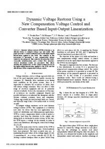
Abstract: This paper discusses the design and development of Dynamic Voltage Restorer (DVR) controller for voltage unbalanced compensation using d-q-o transformation technique. The controller in d-q-o coordinates has better performance than conventional controllers. The controlled variables in d-q-o coordinates are then inversely transformed to the original voltages which produced reference voltages to a DVR. The performance of proposed control algorithm has been simulated by MATLAB/SIMULINK SimPower System Toolbox. A prototype has been developed in order to validate the effectiveness of the proposed control solution. Simulation and experimental results are presented for various conditions of disturbances in the network included unbalance voltage in the supply voltage to show the compensation effectiveness. Key words: Controller % Dynamic voltage restorer % Voltage unbalance % Matlab/Simulink % D-q-o coordinate % Disturbances INTRODUCTION Several methods are available to prevent equipment mal operation due to voltage sags. The two obvious solutions, at first sight, are a reduction of the number of faults and improvement of equipment immunity. However, experience has shown that in many practical cases neither of these methods is suitable. The most common mitigation method remains the installation of additional equipment between the power system and the equipment, either directly with the equipment terminals or at the customerutility interface. The uninterruptable power supply (UPS) has traditionally been the method of choice for small power, single-phase equipment. For large equipment several methods are in use and under development, one of which is the series voltage controller, also known under the name “Dynamic Voltage Restorer” or DVR [1-4]. The Dynamic Voltage Restorer (DVR) is a series custom power device intended to protect sensitive loads from the effects of voltage sags at the point of common coupling (PCC).A typical DVR connected system circuit is shown in Figure 1, where the DVR consists of essentially a series connected injection transformer, a voltage source inverter (VSI), inverter output filter and an energy storage device connected to the dc-link. The power system upstream to DVR is represented by an equivalent voltage source and source impedance. The
basic operation principle of the DVR is to inject an appropriate voltage quantity in series with the supply through an injection transformer when PCC voltage sag is detected. Loads connected downstream are thus protected from the PCC voltage sag [5-6]. The voltage sags as defined by IEEE Standard 1159, IEEE Recommended Practice for Monitoring Electric Power Quality, is “a decrease in RMS voltage or current at the power frequency for durations from 0.5 cycles to 1 minute, reported as the remaining voltage”. Typical values are between 0.1 p.u. and 0.9 p.u. and typical fault clearing times range from three to thirty cycles depending on the fault current magnitude and the type of over current detection and interruption [7]. The details of the existing controllers has been applied in DVR can be found in [8-11]. In this paper, the improvement of d-q-o technique strategy is applied to the control of a three phase DVR. The proposed of the control strategy has the following advantages compared to the existing ones. The improvement of the controller is easy to design and does not much depend to circuit parameters. The dc value of the capacitor and harmonic ripple current due to input power circuit can be reduced. The controller can detect any disturbance in the network very fast. Once the disturbance is detected, the DVR act very quickly in order to correct it and injecting the exact amount of energy required.
Corresponding Author: Rosli Omar, Faculty of Electrical, University Teknikal Malaysia Melaka, Ayer Keroh, Melaka 75450, Malaysia, E-mail:
[email protected].
1480
World Appl. Sci. J., 10(12): 1480-1489, 2010
special attention must be paid on two types of configuration namely: C C
Fig. 1: Typical Existing DVR circuit topology
Fig. 2: Symmetrical components of unbalanced system of voltages The Concept of Voltage Unbalance Using Dynamic Voltage Restorer: Figure 1 shows a distribution system which consists of feeder A, feeder B and feeder C. A DVR is connected in series between sensitive loads in order to mitigate unbalanced loads or faults in feeder A or B. The possibility of compensation of voltage unbalance can be limited by a number of factors including finite DVR, power rating, different load conditions, background power quality problems and different types of sags [12-13]. Figure 2 shows the symmetrical components of an unbalanced system of voltages. These are called positive sequence, negative and zero sequence systems. For a perfect balanced system both negative and zero sequence systems would be absent. Proposed New Configurations Circuit of Dvr Main Circuit of New Configurations: Figure 4 illustrates a new configuration model of the proposed DVR system and the system consists of a DC voltage source (Vdc), three single phase injection transformer, a three phase voltage source PWM inverter, L-C output filter and sensitive loads. In this proposed designed of DVR,
Filtering Configuration Injection transformer winding
Filtering configuration for DVR is very important as it related with the system dynamic response. The filtering system of the DVR can be placed either on the high voltage or the low-voltage side of the injection transformer and are referred to as line side filter [14-15] and inverter-side filter [15-18] respectively. In the proposed filtering system as shown in Figure 3, the filtering scheme is installed for both on the low and high voltages. The filter inductor, capacitor and resistor (Lfa,Lfb,Lfc, Cfa,Cfb,Cfc and Ra,Rb,Rc) are installed on low voltage side between the series converter and the transformer and the high voltage side(C1,C2 and C3), when it is place in low voltage side, high order harmonics from the three phase voltage source PWM inverter is by pass by the filtering scheme and its impact on the injection current rating can be ignored. The type of this filtering configuration can also eliminate switching ripples produced by the converter. As for the filtering scheme is placed in the high voltage side in this case, high order harmonic currents will penetrates through the injection and it will carry the harmonic voltages. When compensate the voltage sags/swells at the critical load, DVR produce a harmonics distortion fed from series transformer as injection voltage to the critical load. Using the FFT analyzer Voltage Total Harmonic Distortion (VTHD) of 1.4% of the filtering scheme is shown in Figure 3 is satisfy the IEEE-519 standard harmonic voltage limit. In DVR the injection transformer must be designed properly according to the voltage required in the secondary side of the transformer. The ratio of the injection transformer will determines the flow of current in the primary side which may affect the performance of the power circuit devices in DVR which consists of Voltage Source Inverter (VSI). The transformer in DVR can be configured either in Delta-open or Wye open winding. In order to step-up the VSI output voltage to mitigate 50% of voltage sags in the distribution system the series injection transformer turn ratio must be calculated. In the proposed configuration as shown in Figure 4, the maximum injection transformer voltage per phase is set to Vinj 1N is equal to 120 Vrms and single phase voltage line to line of VSL is about VVSI L-L = 60 V. The comparison of two types of transformers can be described as follow;
1481
World Appl. Sci. J., 10(12): 1480-1489, 2010
Fig. 3: THD for voltage of the proposed scheme
Fig. 4: New Configuration of DVR The turn ratio of the injection transformer In Delta -Open winding aDelta − open =
Vinj1φ VVSI ( L − L )
=
If in case the injection transformer is connected in Wye -Open winding
120V =2 60V
aWye −Open =
1482
Vinj1φ VVSI ( L − L )
=
(
3 Vinj −1φ
)=
VVSI ( L − L ) 1φ
3 (120 ) 60
= 3.4
World Appl. Sci. J., 10(12): 1480-1489, 2010 Vdc ref Vdc
+-
PI CONTROLLER
LPF
Block 1
Block 5 VLd
+ +
Vq ref Vquadrature
Unbalanced Voltage Detection
V sc ref
θ
Vq dc
θ
V sa ref
LPF
++
V sb ref
VLq
Vd ref
-o d-q
VLc
LPF
Vd dc
ab c
VLb
a bc d- q -o
VLa
Block 4
Block 6
Vsc Block 2 Vsa Vsb Vsc
Vs
PI
Amplitude
+ Block 3 THREE PHASE PLL
Vs REF
PWM Controller
Vsb Vsa
C O N T R O L L E R
PWM1 to PWM6 switches
θ
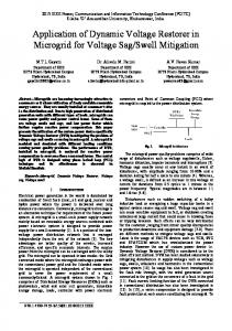
Fig. 5: Block Diagram Control of the proposed Scheme of DVR for Unbalanced Voltage Based on the calculation the high ratio of the transformer winding will increase the primary side current, so in the proposed configuration the wye-open winding is used. Control Method of the Proposed Scheme: There are many control schemes reported in the literature for control of DVR such as instantaneous reactive power theory, power balanced theory, synchronous reference frame theory etc [14]. In this paper a new control method for DVR system is proposed by using the d-q-o transformation or Park’s transformation for sags/swells detection. The d-q-o method gives the sag depth and phase shift information with start and end times. The main aspects of the control system are shown in Figure 5 and include the following blocks:
C
Block 1 is used to convert the three phase load voltages (VLa, VLb, VLc ) into the "-$-o coordinates as in equation (1) Vα VLa V = Q β VLb V VLc o
−1 1 2 2 3 Where Q = 0 3 2 1 1 2 2
1483
−1 2 − 3 2 1 2
(1)
World Appl. Sci. J., 10(12): 1480-1489, 2010
C
C
Block 1 is used to convert the three phase load voltages (VLa, VLb, VLc ) into the "-$-o coordinates as in equation (1), the three phase load voltages reference components V"-ref, V"-ref and Vo ref can be converted to Vd ref and Vq ref (2). cos θ Vd 2 = Vq 3 sin θ
sin θ cos θ
Vα Vβ
(2)
sin θ cos θ
Vd Vq
(3)
Transformation to dqo to abc cos θ V α 2 = Vβ 3 sin θ 1 Va Vb = −0.5 Vc −0.5
C
C
C
3 2 3 2
(4)
Block 2 is considered as a source voltages (Vsa, Vsb, Vsc). The amplitude of AC voltage at the sources (Vsource) can be calculated as follow; 2 Vsource = 3
C
1 Vα 1 Vβ V o 1
0
(Vsa )2
+ (Vsb )
2
2 + (Vsc )
(5)
Block 3 is a three phase PLL (Phase-locked loop). The angle 2 of the source voltage can be obtained using three phase PLL. The information extracted from the PLL is used for detection and reference voltage generation. Block 4 is the detection scheme for the voltage Unbalanced compensator. From Figure 5 shows that, the synchronous frame variables, Vd and Vq are used as inputs for low pass filters to generate voltage references in the synchronous frame. Block 5 receive the components of the load voltage vectors Vd ref and Vq ref and transforms them to three phase coordinates using equation (3) and (4) the generation voltages are used as the voltage reference. The DC link error in Figure 5 is used to get optimized controller output signal because the energy on the DC link will be changed during the unbalance voltage.
Block 6 is the PWM block, this block provides the firing for the Inverter switches (PWM1 to PWM6). The injection voltage is generated according to the difference between the reference load voltage and the supply voltage and is applied to the voltage source converter (VSC).
Simulation Results: The proposed control scheme for the DVR is validated in this section via MATLAB/SIMULINK SimPower System toolbox. In this paper, the load is represented by a series equivalent rated at 200V, 5KVA at 0.9 load power factor. A simulation model has been developed in MATLAB/SIMULINK as shown in Figure 4. Simulation and experimental parameters are given in Table 1. The performance of the DVR for different supply disturbances is tested under various operating conditions. Several simulation of the DVR with proposed controller scheme and new configuration of it have been made. Figure 6 shows that unbalanced output voltages, positive sequence, negative and zero sequence. In case of zero sequence all phases are equal. The distortions occur for both the negative and zero sequence during transformation processes from stationary abc reference frame to d-q-o coordinates. In figure 6 (c) also shows that the negative sequence disturbances rotates in the opposite direction. Experimental Results: In order to validate the effectiveness of the proposed system a small scale prototype of DVR was built and tested. The prototype developed based on schematic in Figure 4, all the system parameters for the hardware designed as shown in Table 1. The prototype is rated to protect 5KVA load 40% voltage sags mitigation and in case of unbalance voltage at the Point of Common Coupling (PCC) is set at 10%20%. Three phase load comprising of 40 S and 60mH inductor. Table 1: System Parameters Proposed Main Supply Voltage per phase
240V
Line Impedance
Ls =0.5mH Rs = 0.1
Series transformer turns ratio
1:1
DC Bus Voltage
120V
Filter Inductance
2mH
Filter capacitance
1uF
Load resistance
40
Load inductance
60mH
Line Frequency
50Hz
Switching Frequency
5kHz
1484
World Appl. Sci. J., 10(12): 1480-1489, 2010
(a)
(b)
(c)
(d)
Fig. 6: (a) Unbalanced voltage, (b) Positive sequence (c) Negative sequence (d) Zero sequence The proposed control strategy is implemented digitally in DSP TMS320F2812. The DSP was selected as it has a 32-b CPU which operating at 150MHz. The voltage and current sources were sent to the analog digital converter of the DSP. The sampling times are governed by the DSP timer called a CpuTimer0 which generates periodic interrupt at each sampling times Ts. The Interrupt Service Routine (ISR) will read the sampling value of the voltage and current source from the analog digital converter (ADC) The DSP controller offers a display function, which monitor the disturbances in the real time. The control algorithm which is proposed in section II is tested with a control using DSP TMS 320F 2812.
The controller has its own ADC converters and PWM pulse outputs. The inputs of a 3-leg Voltage Source Converter (VSC) are the PWM pulses which are generated by the digital controller. The three phase supply voltage is measured continuously and it then compared with the reference voltage in order to regulate load voltage response. If there any disturbances occur, different between the supply voltage and load voltage, the different voltage between them will be compensated. The amount of compensated voltage needs to be injected is calculated and the results of the supply, load and compensated voltages will be processed by the DSP and injected to the IGBT switching scheme (PWM1 to
1485
World Appl. Sci. J., 10(12): 1480-1489, 2010
PWM2). Positive and negative sequence can be converted when three voltages are sensed in phase and quadrature components. The conversion process of positive and negative sequence can be formulated using equations (6) - (7). 2π 2π sin θ t sin θ t − sin θ t + Vsa Vd ( pos ) 2 3 3 = Vsb Vq ( pos ) 3 cos θ t cos θ t − 2π cos θ t + 2π ( ) V 3 3 sc
(6)
Vd (neg ) Vq (neg )
2π 2π sin θ t sin θ t + sin θ t − Vsa 2 3 3 = Vsb 3 cos θ t cos θ t + 2π cos θ t − 2π ( ) V 3 3 sc
(7)
(a)
(b)
(c)
(d)
In the prototype developed the maximum sags time is set to 100 ms as it very fast to detect any disturbances occur in the network. It should be mentioned that with the new configuration of the topology and an improvement of the proposed controller also can detect voltage swells in the network. Voltage swells can occur more frequently than other power quality phenomenon and is known as the most important power quality problems in the power distribution system. In normal situation if there is no voltage swells detects in the network, the dc-link capacitor charging current is almost zero. Supply current of the network is equal to load current which is sinusoidal. When the DVR detect the voltage swells, the DVR starts to inject an appropriate voltage for the voltage swells; active power is supplied from the dc-link to the network which causes dc-link voltage to drop. So the controller will compared with the reference voltage and inject missing voltage through injection transformer. The three phase 20% balance voltage.
Fig. 7: (a) Unbalanced voltage, (b) Positive sequence (c) Negative sequence (d) Zero sequence 1486
World Appl. Sci. J., 10(12): 1480-1489, 2010
(a)
(b)
(c) Fig. 8: (a)Three phase Unbalanced Voltages (b) Injected Voltages (c) Restoration load Voltages
(a)
(b)
Fig. 9: (a)Total Harmonic Distortion Current (THDI) under unstable dc-link (b) Total Harmonic Distortion Current (THDI) under stable dc-link 1487
World Appl. Sci. J., 10(12): 1480-1489, 2010
(a)
(b)
(c) Fig. 10: (a)Three phase 20% balance Voltages Swells (b) Injected Voltages swells (c) Restoration load Voltages Can be observed in Figure 10(a), the DVR will detect voltage swells and injects the missing voltage as shown in Figure 10(b). The fast response to detect voltage swells by the controller will causes the load voltage is secured from distortion and this can be illustrated in Figure 10(c). The performance during 10%-20% voltage unbalance is illustrated in Figures 7(a). In Figure 7(b), (c) and (d) shows that positive sequence, negative and zero sequence. Next, the performance of DVR for a three phases to ground fault is also investigated. Figure 8 (a) shows that unbalanced three phases fault. Injection voltages produced by DVR is shown in Figure 8(b). Figure 8(c) shows the load voltages restoration using DVR. From the results show that the load terminal voltage is restored and help to maintain a balanced and constant load voltage. In new configuration of the proposed system, the DC link capacitor acts as an energy storage element of the DVR.The DC link of the DVR prototype is determined
based on the rating of the IGBT. Harmonic current is depending on the DC link voltage. DC side capacitor Cdc1 and Cdc2 should be large enough to absord the ripple without the distorting the dc bus voltage much. If there is distortion in the dc voltage the inverter output will get distorted with third harmonic content. With the stability of the DC bus and the Total Harmonic Distortion for current (THDI) for third harmonics current is reduced 7.8 % to 2.8% as shown in Figures 9(a) and 9(b). CONCLUSION In this research the new configuration of the DVR prototype has been proposed. The proposed topology is capable to mitigate various disturbances in the network. A control system based on improvement d-q-o controller has been applied to the prototype. The effectiveness of the proposed configuration and improvement of d-q-o controller can be seen from Simulation and experimental
1488
World Appl. Sci. J., 10(12): 1480-1489, 2010
results. The implementation of a DSP TMS320F2812 based on DVR to extract positive and negative sequence was discussed. The experimental results show that the performance of the DSP controller is satisfactory in mitigating disturbances in the network such as voltage sags, swells and unbalance voltage in low voltage distribution system.
9.
ACKNOWLEDGEMENT
11.
10.
The authors wish to thank UM and UTeM for providing grant under grant PS002/2007B for this project. 12. 1.
2.
3.
4.
5.
6.
7.
8.
REFERENCES IEEE Standards Board, 1995. IEEE Std. 1159-1995, IEEE Recommended Practice for Monitoring Electric Power Quality. IEEE Inc. New York. Sabin, D., 1996. An assessment of distribution system power quality, Elect. Power Res. Inst., Palo Alto, CA, EPRI Final Rep. TR-106294-V2, vol. 2, Statisticalbb Summary Report. Fitzer, C., M. Barnes and P. Green, 2004. Voltage Sag Detection Technique for a Dynamic Voltage Restorer, IEEE Trans. On Industry Application, 40(1). Vilathgamuwa, M., A.A.D. Ranjith Pcrcra and S.S Choi, 2002. Performance improvement of the dynamic voltage restorer with closed-loop load voltage and current-mode control, IEEE Transactions on Power Electronics, 17(5): 824-834. Elnady, A. and M.M.A. Salama, 2005. Mitigation of Voltage Disturbances Using Adaptive PerceptronBased Control Algorithm, IEEE Transactions on Power Delivery, 20(1): 309-318. Nielsen, J.G., M. Newman, H. Nielsen and F. Bilabjerg, 2004. Control and Testing of a Dynamic Voltage Restorer(DVR) at medium voltage level’, IEEE Transactions on Power Electronics, 19(3): 806-813. Mekri, F. and B. Mazari, 2006. Machmoum, Control and optimization of shunt active power filter parameters by fuzzy logic, Can. J. Electr. Comp. Eng., 31(3): 127-134. Vazquez, J.R. and P. Salmeron, 2003. Active Power Filter Control Using Neural Network Technologies, IEE Procedings -Electric Power Applications, 150(2): 139-145.
13.
14.
15.
16.
17.
18.
1489
Madtharad, C., 2002. Premrudeeprceechacharn, Active Power Filter for Three-Phase Four-Wire Electric System Using Neural Networks Electric Power Systems Res., 60(1): 179-192. Jain, S.K., P. Agrawal and H.O. Gupta, 2002. Fuzzy Logic Controlled Shunt Active Power Filter for Power Quality Improvement, IEE Procedings-Electric Power Applications, 149(3): 317-328. Chung, Y.I., D.J. Won, S.Y. Park, S.I. Moon and J.K. Park, 2003. The DC Link Energy Control Method in Dynamic Voltage Restorer System’, Electrical Power and Energy Systems, 25: 525-531. Mekri, F., M. Machmoum, B. Mazari and N. Ait Ahmed, 2007. Determination of voltage references for series active power filter based on robust PLL system, in: Conference CD-ROM IEEE International Symposium on Industrial Electronics, ISIE, Spain. Han, B., B. Bae, H. Kim and S. Baek, 2006. Combined Operation of Unified Power Quality Conditioner with Distributed Generation, IEEE Trans. On Power Delivery, 21(1): 330-338. Choi, S., B. Li and D. Vilathaguwa, 2002. Design and Analysis of the inverter side Filter used in the Dynamic Voltage Restorer (DVR), IEEE Trans. On Power Delivery, 17(6): 1058-1066. Fornani, F., R. Procopio and M.J.H. Bollen, 2005. SSS compensation capability for unbalance voltage sags, IEEE Trans. On Power Delivery, 20(3): 2030-2037. Stephen, W., E. Middlekauff and Randolph Collins, Jr., 1998. System and Customer Impact: Consideration for series Custom Power Devices, IEEE Trans On Power Delivery, 13(1): 278-282. Awad, H., H. Nelsen, F. Blaabjerg and M.J. Newman, 2005. Operation of static series compensator under distorted utility conditions, IEEE Trans. Power System, 20(1): 1744-1753. Maria Isabel Milands, Enrique Romero Cadaval and Fermin Barrero Gonzalez, 2007. Comparison of Control Strategies for shunt Active Power Filters in Three Phase Four-Wire Systems IEEE Trans. On Power Electronics, 22(1): 229-236.