Advanced Computing, Mohali, India. Jalandhar, India. Amritsar, India. Abstract-This paper proposes a low power Linear. Feedback Shift Register (LFSR) for Test ...
2009 IEEE International Advance Computing Conference (IACC 2009) Patiala, India, 6-7 March 2009
Power Optimization of Linear Feedback Shift Register (LFSR) for Low Power BIST Balwinder Singh VLSI & Embedded System Design Centre for Development Of
Advanced Computing, Mohali, India
Arun Khosla ECE Department, Dr.B.R.Ambedkar National Institute of Technology, Jalandhar, India
Abstract-This paper proposes a low power Linear Feedback Shift Register (LFSR) for Test Pattern Generation (TPG) technique with reducing power dissipation during testing. The correlations between the consecutive patterns are higher during normal mode than during testing. The proposed approach uses the concept of reducing the transitions in the test pattern generated by conventional LFSR. The transition is reduced by increasing the correlation between the successive bits. The simulation result show that the interrupt controller benchmark circuit's testing power is reduced by 46%with respect to the power consumed during the testing carried by conventional LFSR. Keywords-LFSR, Optimization, LowPower,TestPattrens
I.
Sukhleen Bindra Electronics Department Guru Nanak Dev University, Amritsar, India
INTRODUCTION
The main challenging areas in VLSI are performance, cost, testing, area, reliability and power. The demand for portable computing devices and communications system are increasing
rapidly. These applications require low power dissipation for VLSI circuits. The power dissipation during test mode is 200% more than in normal mode [1]. Hence it is important aspect to optimize power during testing. Power optimization is one of the main challenges. There are various factors that affect the cost of chip like
packaging, application, testing etc. In VLSI, according to
thumb rule 5000 of the total integrated circuits cost is due to
o.1 ooi1
cost: cents !tansistor transistor
01
T
i.T OXI 0000 1982
prot
al ns Based on 97 SIA
1985 188 1991
9
9
2
2003
Roadmap Dat 2006 2009
220l2
Figure 1: Fabrication cost versus testing cost
There are main two sources of power dissipation in digital circuits; these are static and dynamic power dissipation. Static power dissipation is mainly due to leakage current and its
contribution to total power dissipation is very small. Dynamic dissipation is due to switching i.e. the power consumed due to short circuit current flow and charging of load
power
P
0.5VDD2E(sw)CLFCLK
where Vdd is supply voltage, E(sw) is the average number of output transitions per 1/fclk, fclk is the clock frequency and CL is the physical capacitance at the output of the gate. Dynamic power dissipation contributed to total power dissipation. From the above equation the dynamic power depends on three parameters: Supply voltage, Clock frequency, Switching activity. To reduce the dynamic power dissipation by using first two parameter only at the expense of circuit performance. But power reduction using the switching activity doesn't derethprfmacofheicu.
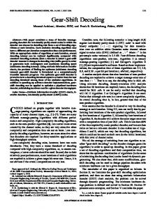
Cost of testing that can't be scaled. * Engineering effort for generating test vectors increases as complexity of circuit increasesderethprfnacofheicu. Power dissipation during the testing is one of most important issue [12]. There are several reasons for this power increased Based on 1997 SIA data, the upper curve shows the in test mode. fabrication cost of transistor and lower curve shows the testing cost of transistor. Figure 1 shows that the fabrication cost transistor decreases over the decades according to Moore's law * To test large circuit, circuits are partitioned to save but the testing cost as constant.[2] the test time but this parallel testing results in excessive energy and power dissipation. *
978-1T-4244-2928-8/09/$25.00 ©& 2009 IEEE
3l11
* *
Due to the lack of at-speed equipment availability, delay is introduced in the circuit during testing. This cause power dissipation. In the successive functional input vectors applied to a give cicuit innonnl mde hve sigifiant givrenlcircuitshin modrelhaveatignifient correlation, testpatns thecan con be twen. consecutive beveryuow Thin cause large during itsavity ino thecircuitn normal test than thatstchtding operation. Poeri cir .i otciongalt issipatcion ativtmy acMOrexcesive sicing r witchin lacivity, e duringtestmaynverespcation,autosil cst,recola ty, pelaterf prormance normal
whil
d
l
p
ti
fr
related problems.
During testing large power is dissipated than in the normal
mode. This is due to lack of correlation between the patteRnsgnrte e (for sucsietesti BISTandthislargepow xalion
tasesting)forlFSRin (frcts:
BIST)andthislargepowerdissipatio cases following effects:
..t inreasednpowerimay rons for rechnoliy, performance veriicton aonomy .an technog restappliated oproblems.sLowcpower is duporiangtest tan deql VLS circuitstdesin important fiueappliaof o iti me in thuay's od beSIcircming
and iS expected to become one of the major objectives in the near future. the near future. * High power and ground noise caused by high switching during testing are serious problem where the supply connects are poor. Thus excessive noise can change the logic state of the circuit lines leading good dies to t.he fail the test and hence loss of yield. rut iSis designed in the deep sub micron *As the circuit small supply voltages and (DSM) technology, this uses ' . . . hence this reduces the use of to special cooling equipment
diAs
*
PRIORWORK
There has been various low power approaches proposed to solve the problem of power dissipation during the testing. Some of the earliest work that has been proposed for the paper. powerOne during testing this optimizing method is toareusediscussed Random inSingle section of the is (RSIC)test test generation, to Input Change generate low power patter. In thiswhich method,used power consumption is reduced but at the additional cost is between 1900 and 130o. Another technique was proposed in [5]. This approach proposed a low transition LFSR for BIST applications. This reduces the average and peak power of circuit during testing. In [6] approach, a fault model and ATPG algorithm is chosen first and then test pattern are generated to obtain the desired fault coverage. There are various advantages of test pattern generation at a higher level than the gate level. While F. Corno et al has proposed for the low power test pattern generation for sequential circuit [7]. In this paper, redundancy is introduced during testing and this reduces the power consumption without affecting the fault coverage. In [8], it is shown that different LFSR architecture affects the power consumed and the hardware used. Jinkyu Lee et al [9] developed a LFSR reseeding scheme. In this there arechain. two goals, firstisistotoreduce reduce the the number number of approach, in scan Second of transition spcfebisgnrtdyLFReedn. LFSR bits
~~~~~~~specified
generated by III.
reseeding.
BIST ARCHITECTURE
It is very important to choose the proper LFSR architecture for the appropriate fault coverage. Every architecture consumes different power even for same polynomial. Another p~~~~~~roblem associated with choosing LFSR iiS LFSR desi n issue .g which includes LFSR partitioning, ing this the LFSR are differentiated on the basis of hardware cost and testing time cs
hendeeposubfmicron.achieving
t h remove werxessive ed.Butinoth Low power testing iS dungatatest. done at at-speed. But in other
testing techniques, circuits are added to lower the frequency of circuit during test.
For complex circuits, hierarchical approach is used. The advantage of hierarchical approach is that every block is tested separately. Test input is given to each block and output is observed and verified. DFT (Design For Testability) is the action of placing features in a chip design process to enhance the ability to generate vectors, achieve a measured quality level or reduce cost of testing. The conventional DFT approaches use scan and BIST. In this paper a modified low power LFSR are used in which the number of transitions of test pattern are reduced testing. The remainder paper is organized as follows: Section 2 describes the previous work while section 3 presents the proposed work. Section 4 describes the simulation results and conclusions.
312
II.
A typical BIST architecture consists of a test pattern generator (TPG), usually implemented as a linear feedback shift register (LFSR), a test response analyzer (TRA), implemented as a multiple input shift register (MISR), and a BIST control unit (BCU), all implemented on the chip (Figure 1). This approach allows applying at-speed tests and eliminates the need for an external tester. The BIST architecture components are given below. * Circuit Under Test (CUT): It is the portion of the circuit
tested in BIST mode. It can be sequential, combinational or a memory. Their Primary Input (PI) and Primary 0
output (P0) delimitmit. Outest Pae Generat (t P Test Pattern Generator (TPG):
It generates the test
microprocessor. The patterns may be generated in psuorno ordtriitcly
2009 IEEE Internlationlal Advance Computing Conference (IACC 2009)
Parttr en Generation
B IST Co ntro Her Unit (B CTJ)
Ciruit Under T est; (CUT)
D
Test Results
Figure 2 BIST Architecture *
*
*
Multiple input signatures registers (MISR): it is designed for signature analysis, which is a technique for data compression. MISR efficiently map different input streams to different signatures with every small probability of alias. MISR are frequently implemented in built-in-self-test (BIST) designs, in which output responses are compressed by MISR. Test Response Analysis (TRA): It analyses the value sequence on PO and compares it with the expected output BIST Controller Unit (BCU): It controls the test execution; it manages the TPG, TRA and reconfigures the CUT and the multiplexer. It is activated by the Normal/Test signal and generates a Go/No go. IV.
1Q
Q
Q
p
F~~~~~~~~~~
~ ~~~
~
~~reset r
r
,
Figure 3: LFSR in which input of first flip-flop is xored with last flip-flop. In this approach the 3 intermediate test vectors are generated between every two successive vectors (say TI, T2). The total number of signal transition occurs between these 5 vectors are equivalent to the number of transition occurs between the 2 vectors. Hence the power consumption is reduced. Additional circuit is used for few logic gates in order to generate 3 intermediate vectors. The 3 intermediate vectors (Ta, Tb, Tc) are achieved by modifying conventional flip-flops outputs and low power outputs. The first level of hierarchy from top to down includes logic circuit design for propagation either the present or next state of flip-flop to second level of hierarchy. Second level of hierarchy is implementing Multiplexed (MUX) function i.e. selecting two states to propagate to output as shown in flow:
F
al i c
gives output as previous
GeneratinggTI Bothhaless axe idle. Firsthalf seondhalf sutputissrb oueis sentsentto itoroutpu.t cutp and|
ALGORITHM FOR LOW POWER LFSR
As discussed in the previous section LFSR is used to generate test patterns for BIST. In this, test patterns are generated
externally by LFSR, which is inexpensive and high speed. LFSR is a circuit consists of flip-flops in series. LFSR is a shift register where output bit is an XOR function of some input bits. The initial value of LFSR is called seed value. LFSR's seed value has a significant effect on energy consumption. [3]. The output that influence the input are called tap. A LFSR is represented by as polynomial, which is also known as characteristic polynomial used to determine the feedback taps, which determine the length of random pattern generation. The output of LFSR is combination of I's and O's. A common clock signal is applied to all flip-flops, which enable the propagation of logical values from input to output of flip-flops. Increasing the correlation between bits reduces the power dissipation. This can be achieved by adding more number of test vectors, which decreases the switching activity. LFSR is characterized by the polynomial by its characteristics polynomial and inverse of characteristics polynomial is generated polynomial.
Q
1> * ty
0- Test Response ArLalysis (TRA)
I
Q
e
Xond
0
Generating next vector
inj e ctor
eneratingTa
Second half is active, and first halfis in idle mo de ard gives same output a previous
O eneratinggTb Both halves are in idle mode. First havees is given byinjector and secondhIf is same as previous
Generating Tc
Figure 4: Proposed algorithm for low power LFSR
2009 IEEE Internlationlal Advance Computing Conference (IACC 2009)
313
The EDA tool is used in which conventional and low power LFSR is coded in Verilog hardware descriptive language and a is seed value given to the (01001010010110101101001O100101101011) polynomial and primitive value polynomial in LFSR block. The outputs of the 36-bit LFSR are used as the inputs to the c432 ISCAS-85 a benchmark circuit of interrupt controller. In this c432 is used as CUT; the generated code is synthesized in Xilinx Web Pack 9.1 for Spartan 2e device. The hardware summary is obtained for each method implementation log file of Xilinx 9.1 project navigator. The RTL view of LP-LFSR with c432 benchmark circuit is shown in figure 5.
|
350
366 256-| 2606 X l5
RFSRl
-LP LFSR
I
166 50
6
input
Dynamic
pcwDer
Output
Dynamic
pcoi'ier
Total power
Figure 6. Comparison of Power dissipation in testing with conventional and low power LFSR rLet isifi: observed that the total power consumed in modified _It LFSR is 46% less than the power consumed with normal LFSR and out put dynamic power is decreased by 44.6 %. It is concluded that low power LFSR is very useful for BIST implementation in which the CUT may be Combinational, sequential and memory circuits. Using low power LFSR technique we can further decrease the power in BIST implementation.
E.
l $--: EU
REFERENCES Figure 5 RTL view of LP-LFSR with C432 benchmark circuit
V.
RESULTS AND CONCLUSION
The results obtained from the Xilinx 9.1 implementation with
the device xc3s200-4pq208 in which, we have generated VCD
file after the post simulation. Xpower is used to calculate the with the simulation files. Results are obtained for each case and comparison of power dissipation is made on the basis of reports is given in table 1 and shown in figure 6. TABLE I. COMPARISON OF POWER DISSIPATION CONVENTIONAL AND LOW POWER LFSR
TYPE Power Vccint(V) Dynamic Quiescent
Vcco33 (V)
Vc3(miV Dynamic Quiescent
Total Power (mW) Battery Capacity (mA) Battery Life (hours)
314
LP-LFSR _________ 1.8 4.42 21.6 3.3
87.6
87.6
6.60 120.22 50 2.27
XORLFSR 1.8 7.39 21.6 3.3
195.3 1.95
6.60 226.54 50 2.11
[1]. E. Atoofian, S. Hatami, Z. Navabi, M. Alisaface and A. Afzali-Kusha," A New Low-Power Scan-Path Architecture," IEEE International
Symposium, Vol.5, pp.5278 - 5281, 23-26 May 2005
[2]. The National Technology Roadmap for Semiconductors Edition. Semiconductor Industry Association.
(ITRS), 1997
[3]. Dr.K.Gunavathi, Mr. K. ParamasivaM, Ms.P.Subashini Lavanya, M.Umamageswaran," A novel BIST TPG for testing of VLSI circuits", IEEE International Conference on Industrial and Information Systems, pp. 8 - 11, August 2006. [4]. Michael L.Bushnell, Vishwani D.Agawal," Essentials of electronic testing for digital, memory and mixed-signal VLSI circuits," Kluwer Academic Publishers, 2000.
[5]. Mohammad Tehranipoor, Mehrdad Nourani, Nisar Ahmed," LowTransition LFSR for BIST-Based Applications," 14th Asian Test Symposium, pp. 138- 143, 18-21 Dec. 2005. [6]. Fulvio Corno, Paolo Prinettom, Matteo Sonzar Eorda "Testability analysis and ATPG on behavioral RT-level VHDL," IEEE International Test Conference, pp 753-759, 1997. [7]. F. Corno, P. Prinetto, M. Rebaudengo, M. Sonza Reorda," A Test Pattern Generation methodology for low power consumption," pp.1-5, 2008. [8] Shilesh Malliyoor, Chao You," Comparison of hardware implementation and power consumption of low-power multiple output linear feedback shift register," Journal of engineering, computing and architecture, 2007. [9. ]Jinkyu Lee and Nur A. Touba," LFSR-Reseeding Scheme Achieving Low-Power dissipation during Test," IEEE transactions on computer-
aided design of integrated circuits and systems, 26(2), February 2007.
[10]Yervant Zorianl, Sujit Dey, Michael J. Rodgers "Test of Future Systemon-Chips"ICCAD 2000 [11] P.Glard et al "Survey 0 F Low-Power Testing Of Vlsi Circuits"IEEE Design & Test Of Computers, vol. 19, no. 3. (2002), pp. 80-90. [12] A. Crouch, "Design-for-Test for Digital IC's and Embedded Core Systems", Prentice Hall, 1999
2009 IEEE Internlationla/Advance Computing Conference (IACC 2009)