architecture design of flexible system-on-a-chip solutions in the digital baseband ... short description of our Matlab simulation environment. Section IV contains ... baseband signal processing level, the W-CDMA terminal unit is required to ...
Dynamically Reconfigurable Solution in the Digital Baseband Processing for Future Mobile Radio Devices Ahmad Alsolaim and Janusz Starzyk Ohio University Electrical and Computer Engineering Athens, OH 45701 USA Fax: ++1 740 593 0007 e-mail: {alsolaim, starzyk}@bobcat.ent.ohiou.edu
Abstract . The focus of the paper is a new parallel and dynamically reconfigurable hardware architecture tailored to wireless mobile handset. Its performance issues and potential are discussed. This paper presents the major challenges in realizing flexible microelectronic system for mobile communication applications. The architecture design of flexible system-on-a-chip solutions in the digital baseband processing for mobile radio devices are also discussed.
I. INTRODUCTION With the introduction of the third generation wireless mobile communication systems, new and interesting challenges for system designer are emerging. The complexity of services coupled with the high data rates requirements is a new addition to the typical complex mobile system design. Third mobile communication system (IMT2000) and the future ones will be expected to realize not only a voice services but also high speed data services with the same high quality as fixed networks [1][2]. Due to the high data rates and low bit error requirements for some of these interactive services, mobile terminal is required to perform in a highly efficient manner. Thus the mobile terminal must provide more flexibility, high performance and less power dissipation. A flexible mobile terminal is a mobile terminal, which is able to adapt to the fast changing of standards, and the introduction of new services. All this is expected from the mobile terminal in addition to smaller size and longer battery life. In the last couple of yeas a huge advancement in the areas of Very Large Scale Integrated circuits (VLSI) design and in the electronic design automation tools, is reflected in much smaller and faster devices, and more complex and productive designs. A System-on-a-Chip (SoC) 0-7803-6661-1/10/$10.00 C2001 IEEE
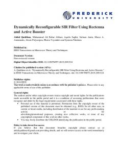
solution for the mobile terminal is proven possible. i.e., the implementation of various functions required by different abstraction layers of a wireless mobile terminal should result in a highly integrated single-chip. A proposed efficient and flexible hardware SoC architecture for digital baseband processing will consist of a mixture of digital signal processors (DSPs) and microcontroller cores, reconfigurable hardware parts, as well as some glue logic and ASIC parts see Fig. 1. The required flexibility will be supported by the inclusion of new coarsegrained dynamically reconfigurable architectures. Since in next generation wireless communication systems a high degree of flexibility is required during operation, dynamically reconfigurable architectures have a great potential to provide this flexibility. At the same time a dynamically reconfigurable architecture can substitute several of today’s ASIC solutions and to move computations from the DSP to the reconfigurable architecture part. The goal is not only to optimize criteria like SoC performance and power, but also to increase the flexibility in order to support a broad range of future mobile applications. The paper is organized as follows. In section II, a brief discussion about the complexity and challenges in the baseband system design of the future generation of mobile devices is presented. Section III will cover in some details the design and operation of our proposed architecture, and short description of our Matlab simulation environment. Section IV contains conclusion.
II. CHALLENGES AND MOTIVATIONS The Wide band Code Division Multiple Access (W-CDMA) is the chosen scheme for the IMT-2000 standard. At the baseband signal processing level, the W-CDMA terminal unit is required to operate with in the following criterion [1]:
.
Low power A/D converters.
.
High speed (more than 100MIPS) and low power CODEC. (MPEG-4) Due to these requirements, different proposed solutions are presented in the literature[1][3][4]. Never the less, all solutions are a temporary fix to part of the problem and there are no comprehensive solutions that consider future systems. The DSP has been the basis of the hardware implementation of digital communication systems for the last fifteen years or more. DSP processors are more suitable to handling algorithms that show a large amount of irregularity in execution. Such irregularity would be in the throughput rates, control flow or frequent branching. On the other hand, programmable logic are well suited for applications such as matched filters, FIR filters, and correlators. The major reason that reconfigurable hardware structures perform better than DSP in such applications is that these application algorithms can be decomposed into many parallel-processing tasks. Each task often involves operations such as Multiplyaccumulate (MAC). And since most DSP offer only single MAC-units, these algorithms must execute serially on DSPs, instead of being executed in parallel in reconfigurable computing. Programmable logic can provide increased system performance at a lower system cost. Programmable logic also combines the flexibility of a general-purpose DSP and the speed, density, and low cost of ASIC solutions. Thus, the enhancement of reconfigurable hardware to a system performance can be two fold: In some applications programmable logic release the DSP processor entirely. In others, programmable logic works concurrently with the DSP processor, off-loading computation-intensive functions, e. g. to save power and to release the DSP processor for other functions.
III. DYNAMICALLY RECONFIGURABLE SOLUTION FOR MOBILE TERMINALS As explained in the preceding section, next generation mobile communication systems will provide the consumer with a large selection of different services, whereas some of them are not known yet. In addition to that, known services have large variety of requirements, for instance, different data rates, different quality of services, and real/non-realtime services etc.. For preparing future to cope with all these challenges, a new coarse-grained and dynamically reconfigurable architecture is proposed. The combination of this application-tailored but flexible hardware architecture and flexible SoCs solutions for the digital baseband
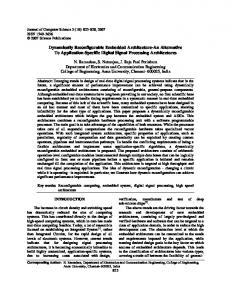
processing will support the efficient realization of the aforementioned features. The proposed Dynamically Reconfigurable Architecture for Mobile Systems (DReAM) consists of an array of parallel operating coarse-grained Reconfigurable Processing Units (RPUs) see Fig. 2. Each RPU is designed to execute all required arithmetic data manipulations for the data-flow oriented mobile application parts, in addition to support necessary control-flow oriented operations see Fig 3. The DReAM array architecture connects all RPUs with reconfigurable local and global communication structures. Additionally, the architecture provides efficient and fast dynamic reconfiguration potential for the RPUs as well as for the interconnection structures, e.g. only in part and during run-time, while other parts of the reconfigurable architecture are active. The decisions during the design of the architecture were based on the careful review of the tailored application area requirements. We started the design of DReAM performing a bottom-up approach by focusing on a list of the most complex and flexibility demanding application parts in future mobile receivers, they are: RAKE-receiver, interpolation filtering, searcher algorithms, coding and modulation techniques. Based on the set of used arithmetic and control-flow operations the performance/power optimized structure design of the RPUs, and of so-called Communication Switching Units (CSUs) was done. As shown in Fig. 2, the DReAM architecture consists of a scalable array of RPUs that have 16-bit fast direct local connections between neighboring RPUs, whereas each four RPU sub-array shares one common Configuration Memory Unit (CMU). The CMU holds configuration data for
Micro-controller
Peripherals.
High speed and low power correlator, for fast cell search
System on a Chip (SoC)
.
Memory
DSP
Dynamically Reconfigurable Architecture.
Figure 1: Proposed System-on-a-Chip solution for future mobile terminals.
performing fast dynamic reconfiguration for each of these four RPUs and is controlled by one responsible CSU. Each CSU controls two CMUs and four global interconnect Switching Boxes (SWB). The detailed hardware structure of the SWBs and the related global as well as local inter-RPU communication mechanisms are described in [5]. The dynamically Reconfigurable Processing Units (RPUs) are the major hardware components of the DReAM architecture for executing the arithmetic data manipulations within application parts of mobile communication systems requiring flexibility, e. g. dynamic hardware reconfiguration. Thus, these application-tailored RPUs perform efficiently the required coarse-grained (8-bit) integer operations needed here. On the contrary, the CLBs (Configurable Logic Blocks) of today’s commercially available fine-grained and general FPGA-chips are operating on the 1-bit level. As shown in Fig. 3, each RPU consists of:
. . . . .
Two dynamically reconfigurable 8-bit data paths, called Reconfigurable Arithmetic Processing Units (RAPs), One Spreading Data Path (SDP), One RPU-controller, Two dual port RAMs, and
One Communication Protocol Controller Each RAP can perform all necessary arithmetic operations (8-bit) identified in the above mentioned examined application parts of mobile communication systems. Each RPU is locally
Communication switching unit.
Configuration memory
Global connection lines
Reconfigurable Processing Unit (RPU)
Fast local connections lines
Dynamic Switching Box Unit
Figure 2: An Overview of the proposed DReAM architecture.
connected to its four neighbors (North, East, South, and West) through 16-bit fast direct connection lines. In addition, it can be connected to the global lines through an SRAMbased dynamic switching box unit (SWB), as shown in Fig 2. The data-driven communication mechanism inside the DREAM array architecture is realized by an asynchronous communication protocol, performed on the 16-bit local and global interconnect lines. The protocol is an efficient handshaking protocol. For local communication between neighboring RPUs a half-interleaved handshake is implemented (1-cycle delay), and for global inter-RPU communication a fully interleaved handshake is used (2-cycle delays). This has to be done due to the difference in length between the local and the global interconnect wires, resulting in different communication signal delays. Each RPU has a Transmitting Unit (TXU) and Receiving Unit (RXU), When an RPU is ready to receive data, a ready signal is sent to the transmitting RPU, followed by an acknowledgment-signal after the receiving RPU have consumed this data. Whenever one RPU cannot consume arriving data, a halt-signal has to be sent to the transmitting RPU to delay the transfer operation until a resume-signal is received. For this reason a 2-bit control line run in addition to every data line so that the TXU in the transmitting RPU and the RXU in the receiving RPU can be synchronized by the halt/resume and ready/acknowledge signals. The global interconnect lines are implemented by two 16-bit lines, running to neighboring SWBs in the way, that each RPU has access to global interconnection. The performance values of these operations for n operation repetitions on a stream of data are provided in Table 1, and are based on a 0.35 µm CMOS standard cell synthesis for the RPU by using a Mietec/Alcatel process. For N repeated operation execution only one configuration set is necessary. The available set of two-input 8-bit operations support either operation with one fixed operand (constant), as well as operations with two variables as inputs.
The Matlab simulation was used to extract the characteristics of the baseband processing algorithms. The Matlab simulation environment is depicted in Fig, 4. The Matlab model for the transceiver was written based on the latest available standards of 3G partner Project (3GPP). As can be seen from the figure, an input format is first transformed to a serial stream of binary bits. Then required baseband processing steps are performed on the data based on the type of service required, for a multimedia service a lower error rate (10e-6) is needed, so compression, CRC coding, and interleaving is applied. A rate matching is then
performed to adjust the data rate to the used transmission rate either by puncturing to reduce the data rate or by repetition to Increase the data rate. Additional signalling bits for the pilot, power control, and frame format are added. The stream of bits is then spited to the I and Q branches. A channelizing Table 1 Performance of all operation implemented in the RPU.
Operation (N repetitions of single operations)
# RAPs used (0.35 µm CMOS)
Number of cycles
2
10*N+1
11.8
2
N+2
100
2
11*N
10.9
Multiply with changing Y Multiply with Fixed Y MAC with changing Y MAC with fixed Y
Freq. [MHz]
IV. CONCLUSION
2
N+2
100
∗
2
N to 43*N
120 to 2.8
Addition
2
N
120
Subtraction
2
N
120
Division
Walsh code is multiplied by the data in a bite-wise fashion.
Input from local connections
Input from Global connections
Input Interface (TXU)
RAP1
Control
RAP2
RAM 2
SDP Unit
RAM 1
Output to Global connections
Figure 3: Block diagram of the RPU.
∗
This paper presents a new dynamically reconfigurable architecture, designed for baseband processing in the mobile terminals were a high flexibility and high data rates are the norm. We presented some of the challenges in the baseband processing requirements, and described the architecture in some detail. An initial performance metrics were also discussed. A Matlab simulation environment, which is used to verify the different steps in the design of the architecture, was presented. Other important characteristics of the architecture are described else were [5]. At this moment the VHDL and Matlab models of the architecture and the mobile transceiver are not finished, but will be available with results at the time of the symposium.
V. REFERANCES [1] S. Kumar, S. Nanda, "High Data-Rate Packet Communications for Cellular Networks Using CDMA: Algorithms and Performance", IEEE J. Select. Areas Commun., vol. 17, pp. 472-485, March 1999 [2] T. Ishika, H. Suzuki. “W-CDMA Hardware-related issues”. International Conf. On Comm. Technology. ICCT’98. Oct. 2224 1998.
Output Interface (RXU)
Output to local connections
A higher layer of scrambling is performed by spreading the data by a scrambling code. This Matlab simulation environment is used throughout the project to verify different steps of development for the proposed DReAM architecture. At this stage, the behavioural and parts of the RTL model of the architecture is almost complete. Results will be presented at the symposium.
Depends on the difference between the operands.
[3] S. K. Knapp,: Using Programmable Logic to Accelerate DSP Functions, Xilinx, Inc. 1995. [4] Stephen D. Lingwood, et al. ”ASIC Implementation of a DirectSequence Spread-Spectrum RAKE-Receiver.”, IEEE 44th Vehicular Technology Conference, 1994. [5] Ahmad Alsolaim, Jürgen Becker, Janusz Starzyk, Manfred Glesner, “Architecture and Application of a Dynamically Reconfigurable Hardware Array for Future Mobile Communication Systems”, IEEE FCCM’00 San Jose 2000. [6] P. Athanas, A. Abbot: Real-Time Image Processing on a Custom Computing Platform, IEEE Computer, vol. 28, no. 2, Feb. 1995. [7] H. Erben, K. Sabatakakis: Advanced software radio architecture for 3rd generation mobile systems., Vehicular Technology Conference, 1998. VTC 98. 48th IEEE Published: 1998 Volume: 2 , Page(s): 825 -829 vol.2
[8] G. R. Goslin, : Using Xilinx FPGAs to Design Custom Digital Signal Processing Devices, Proc. of 1995 DSPx Technical Program, pp. 595-604.
chip, it Computer Design, pp. 49-62, Nov. 1997. [13] David Nicklin :Utilising FPGAs in Re-configurable Basestations And Software Radios, Xilinx Inc. Electronic Eng. Mag.
[9] Mitola.: The software Radio Architecture., IEEE Communication Mag. , May 1995, pp. 26-38.
[14]
Xilinx Corp.: http://www.xilinx.com/products/virtex.htm.
[10] M. Zorzi: Energy Management in Personal Communications and Mobile Computing, IEEE Personal Communications, vol. 5, June 1998.
[15] Jhong Sam Lee, et al.,.: CDMA Systems Engineering Handbook.., Artech House, Boston. 1998.
[11] A. Chockalingam, M. Zorzi, L. B. Milstein, and P. Venkataram, Performance of a Wireless Access Protocol on Correlated Rayleigh-Fading Channels with Capture, IEEE Trans. Communications, vol. 46, no. 5, pp. 644-655, May 1998.
[16] Peter Jung, Joerg Plechinger., “M-GOLD: a multimode basband platform for future mobile terminals”,CTMC'99, IEEE International Conference on Communications, Vancouver, June 1999.
B. Tuck, Integrating IP blocks to create a system-on-a-
Walsh Code Text
Scrambling code
QPSK Modulation
I RRC Filter
Image
Binary Data
Multimedia
Compression
Q Walsh Code
CRC Interleaving
RRC Filter
Add additional bits: • Pilot • Frame format • Power command
De-Compression
De-Interleaving
Walsh Code
QPSK Modulation
For simplicity, A/D, D/A, RAKE, Synchronization, and Channel estimation are omitted for simplicity.
Rate Matching
CRC
Scrambling code
Channel
[12]
Scrambling code
QPSK Modulation
I RRC Filter
Rate Matching
RRC Filter
LPF
LPF
Q Walsh Code
Scrambling code
Figure 4: A block diagram of the Matlab simulation environment.
QPSK Modulation