FPGA-Based Digital Pulse Width Modulator With Optimized Linearity Martin Scharrer, Mark Halton and Tony Scanlan Dept. Electronic and Computer Engineering, University of Limerick Limerick, Ireland Email:
[email protected]
Abstract—This paper proposes a new FPGA based architecture for digital pulse width modulators which takes advantage of dedicated digital clock manager (DCM) blocks present in modern FPGAs and applies manual placement techniques to match internal delays for high linearity. The proposed hybrid DPWM uses a synchronous counterbased coarse-resolution block and a DCM based fine-resolution block implementing a synchronous delay line. The design was successfully implemented on a low-cost Xilinx Spartan-3 FPGA with 9-bit resolution with a switching frequency of 1 MHz. Linearity was manually optimized using the presented technique which reduced the integral non-linearity error by 0.5 LSB.
I. I NTRODUCTION Recent years has seen increased interest in digital control of switched mode power supplies (SMPS) [1–3]. A key reason for this is that digital control has a number of advantages over analog control: such as programmability, reduced sensitivity to external influences, the use of adaptive or other advanced control algorithms along with simpler implementations and prototyping. A digital controller uses a digital pulse width modulator (DPWM) to generate the control signals for the power supply switches. A sufficiently high resolution of the DPWM is critical for the stability of the output voltage. Conversely, a DPWM resolution that is lower than an ADC resolution leads to limit cycling [4, 5]. While DPWMs can be simply implemented using a counter and a comparator, this design leads to unreasonably high clock demands for higher resolutions. In order to implement a N -bit DPWM for a switching frequency of fsw , a clock frequency of 2N fsw is needed. For modern switching frequencies e.g. 1 MHz, a 10-bit counter-based DPWM would have to be clocked at over 1 GHz which can cause design difficulties and increased power consumption. To overcome this problem different architectures have been proposed and implemented in ICs [6–8]. A common architecture is the use of an asynchronous delay line in combination with a large multiplexer (MUX). Both can be combined as a hybrid architecture using a counter for the coarse and an additional short delay line for the fine resolution [9]. This architecture suffers from the difficulty of matching the delay times with the counter period. All delay times must be
978-1-422-2812-0/09/$25.00 ©2009 IEEE
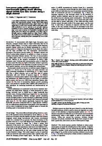
identical and fit exactly between two counter time steps in order to avoid non-linear errors and non-monotonic behavior. While most DPWM implementations target application specific integrated circuits (ASICs), practicing engineers extensively utilize field programmable gate arrays (FPGAs) to prototype and validate their designs. DPWM implemented on FPGAs [10–14] offer the possibility for easy and fast prototyping of SMPSs but the use of pre-existing logic cells and automatic place & route decreases the layout freedom and makes the accurate implementation of the delay line a challenge. II. P ROPOSED DPWM A RCHITECTURES This paper proposes a new FPGA based architecture for digital pulse width modulators which takes advantage of dedicated digital clock manager (DCM) blocks present in modern FPGAs. A DCM as implemented in Xilinx FPGAs is a dedicated configurable all-digital block which can be used to multiply or divide an input clock and to produce multiple phase-shifted versions of it. The feature range includes: multiply by 2, multiply by M=N where M = 2::32; N = 1::32 and four phase output with 0 , 90 , 180 and 270 phase shifts. In addition, DCMs can be cascaded to produce combinations, e.g. multiply by 3=2 with four phases. The proposed hybrid architecture is shown in Fig. 1 and contains a coarse resolution counter-comparator DPWM stage with the bit width of Ncounter . This uses the most significant bits (MSBs) of the Ntotal -bit wide duty cycle as input where Ncounter = Ntotal 2. These MSBs are compared against the counter value. The output pulse of this first stage is delayed using the three phase-shifted clocks from the DCM. The two least significant bits (LSBs) of the duty cycle are used to select one of these four pulses. The final pulse is generated by a set/reset flip-flop (SR-FF) with the coarse pulse used as dominant set input and the selected delayed pulse as negative reset input. A. Coarse DPWM The coarse DPWM shown in Fig. 1 consists of the following blocks: 1) Counter: A simple synchronous counter with Ncounter bits which counts up at every positive clock edge is implemented using a Ncounter bit wide register and an adder.
1220
counter match
DFF CE
DFF
Ntotal
Duty Cycle Comparator
MSBs
Ncounter
CE
Delay Line
Coarse DPWM
2 2 LSBs
coarse pulse Pulse Logic
2
Coarse Pulse Reg
final pulse set
>= 90° Counter
DFF
Counter full Comparator
Ncounter bit
180°
counter full
counter zero
270°
=
all’1s
DFF
M U X
RSFF reset
DFF
DFF
0°
On-Board Clock 50Mhz
DCM
100Mhz
x2
DCM
DCM
128Mhz
x32/25
Fig. 1.
4 phase
Proposed FPGA based DPWM architecture.
2) Comparators: Two comparators with the same bit width as the counter are included. The first produces a counter match signal which indicates if the counter is greater or equal to the Ncounter MSBs of the duty cycle. The second comparator produces a counter full signal which indicates if the counter is full, i.e. all-1s, and will overrun to zero at the next clock edge. A counter zero signal is generated by delaying the counter full signal by one clock cycle using a DFF. 3) Interface Registers: The duty cycle which is calculated outside the DPWM by e.g. a digital signal processor must be held constant during the full pulse length and only be updated directly before the pulse start. This is ensured by the use of interface registers which are only clocked when the counter full signal is high. The two LSBs of the duty cycle which are used as select signal of the MUX need to be delayed by another clock edge to synchronise them with the coarse pulse register. 4) Coarse Pulse Logic and Register: The coarse pulse register is controlled by the counter zero, counter match and the previous register value where the following logic applies: IF counter match == HIGH: coarse pulse reg