Three-Dimensional Space Vector Modulation in abc Coordinates for FourLeg Voltage Source Converters Manuel A. Perales1, M. M. Prats1, Ramón Portillo1, José L. Mora1, José I. León1 and Leopoldo G. Franquelo1, IEEE Senior Member 1
Dept. of electronic engineering. University of Seville, SPAIN.
Corresponding Author: •
Mr. Manuel A. Perales
•
Postal address: Camino de los Descubrimientos s/n. Escuela Sup. De Ingenieros. Dept. de Ingeniería Electrónica. Isla de la Cartuja, 41092. Sevilla. SPAIN
•
Phone number: +34 5 4487374
•
Fax: +34 5 4487373
•
e-mail:
[email protected] This paper has not been presented yet at a conference.
Abstract: Four-leg inverters have been selected as one of the preferred power converter topologies for applications that require a precise control of neutral current, like active filters. The main advantage of this topology lies in an extended range for the zero sequence voltages and currents. However, the addition of a fourth leg extends the space vectors from two to three dimensions, making the selection of the modulation vectors more complex. Most of the algorithms that deal with this problem require an αβγ transformation. This paper presents a new space vector modulation algorithm using abc coordinates (the phase voltages) avoiding the αβγ transformation. Thanks to the use of abc coordinates, the algorithm is much simpler and more intuitive than in αβγ representation, drastically reducing the complexity of modulation algorithm and the computational load associated to it. Index Terms- Four-leg voltage source converter, three-phase four-wire, 3D-space vector modulation, active filter.
I. INTRODUCTION In recent years, the 4-leg topology for 3-phase+neutral inverters have been used in many applications, such as controlled rectifiers [1], active power filters [2][7], and, in general, in applications that require a precise neutral current control. This topology, shown in Fig. 1-a, presents the advantage of adding an extra degree of freedom, expanding the control capabilities of the inverter using the same dclink capacitors and voltages compared with the other classic topology that uses a split capacitor inverter with three leg, as can be seen in Fig. 1-b. On the other hand, the addition of the fourth leg also increases the complexity of the phase voltage control. This is due to the fact that in this configuration, the phase voltages are not decoupled as in the split capacitor topology, forcing the use of three-dimensional space vector modulation (3D-SVM) techniques.
sa
sb
sa va
sc
sb vb
sf
sc vc
sf
+ -
vf (a)
sa
sb
sc
sa
sb
sc
+ Vdc 2 + Vdc 2 -
Vdc
va
vb
vf
vc (b)
Fig. 1. Simplified diagrams of classical 4 wire topologies. (a): 4-wire 4-leg topology; (b): 4-wire 3-leg with split capacitor topology.
Most papers dealing with the 3D-SVM use a representation of
voltage vectors in αβγ
coordinates[1][3][8][9], instead of using abc coordinates. This representation offers an interesting information about the zero sequence component of both currents and voltages (proportional to the γ coordinate), however it has some drawbacks: •
First of all, the change of reference frame has to be carried out, implying complex calculations.
•
The three-dimensional representation of the switching vectors, in αβγ is difficult to understand, not offering a clear picture of the vector positions in the space. This is worse in a multilevel configuration, and it will be shown that in abc coordinates it is more clear.
•
Most methods based on αβγ representation need to determine the “sextant” in which the desired voltage vector is included, which leads to many complicated operations, including rotations, complex comparisons and so forth. The change from the abc to the αβγ reference plane probably responds to historical meanings
more than to practical considerations in most cases. It seems to be the easiest way to extend the plane case, in which the αβ reference frame really simplifies the problem. But it is not necessary at all. In this paper, a 3D-SVM method expressed in abc coordinates is presented. It greatly simplifies the selection of the tetrahedron that contains a given voltage vector, and can be easily extended to a multilevel inverter, with n voltage levels. After this introduction, In Section II the graphical representation of the 3D voltage vectors in abc coordinates is presented, extracting some important conclusions for the further sections. Next, the method for choosing the tetrahedron containing a given voltage vector is presented, showing its extreme simplicity in terms of real time calculations. Then, in Section IV, some experimental and simulation results of the four-leg inverter using this 3D-SVM technique are presented and discussed. Finally, in Section V some conclusions and future lines are pointed out. The main target of this paper is to prove the extreme simplicity of the representation in abc coordinates, offering a complete solution for the four-leg 2-level inverter and an easy way to extend the method to n-level 4-leg inverters.
II. FOUR-LEG INVERTER VOLTAGES IN abc COORDINATES The four-leg inverter phase-neutral voltages, (vaf vbf vcf) are decoupled, having to be expressed in a three-dimensional space. For doing this representation, we choose these phase voltages, vaf, vbf and vcf as our reference frame. Then, the switching vectors present a very simple and straightforward expression (1), that depends on the discrete functions si. These functions are directly the gating signals of the upper switch of each branch, with values {0, 1} depending on whether or not the lower or upper switch of the i leg is connected, as it is depicted in fig. 1-a. Note that dead times are not considered in this approach. ⎡va − v f ⎤ ⎡ sa − s f ⎤ ⎢ ⎥ ⎢ ⎥ vabc = ⎢ vb − v f ⎥ = VDC ⎢ sb − s f ⎥ ⎢ vc − v f ⎥ ⎢ sc − s f ⎥ ⎣ ⎦ ⎣ ⎦
(1)
In Table I, the sixteen switching combinations of the inverter are presented, showing the expression of switching vectors in abc coordinates. To simplify the notation, the vectors are normalized dividing them with VDC.
TABLE I. SWITCHING STATES ,VOLTAGE TERMINALS AND SWITCHING VECTORS IN ABC COORDINATES
State 1 2 3 4 5 6 7 8 9 10 11 12 13 14 15 16
sf 0 0 0 0 0 0 0 0 1 1 1 1 1 1 1 1
sa 0 0 0 0 1 1 1 1 0 0 0 0 1 1 1 1
sb 0 0 1 1 0 0 1 1 0 0 1 1 0 0 1 1
sc 0 1 0 1 0 1 0 1 0 1 0 1 0 1 0 1
vaf 0 0 0 0 1 1 1 1 -1 -1 -1 -1 0 0 0 0
vbf 0 0 1 1 0 0 1 1 -1 -1 0 0 -1 -1 0 0
vcf 0 1 0 1 0 1 0 1 -1 0 -1 0 -1 0 -1 0
Vector V1 V2 V3 V4 V5 V6 V7 V8 V9 V10 V11 V12 V13 V14 V15 V16
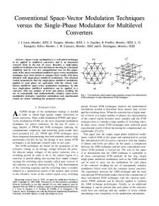
Fig. 2. Dodecahedron that contains the control region, in abc coordinates, showing the switching vectors
Using this representation, it is very easy to notice that the vectors are all in the vertices of two cubes, with an edge length of one: one of them is placed in the “all positive” region (vectors 1 to 8) and the other one is in the “all negative” region of the space defined (vectors 9 to 16), as represented in Fig. 2. The common vertex of both cubes represents, precisely, the zero voltage double vector (vectors 1 and 16). Joining the corresponding vertices of the two cubes, the region included in this dodecahedron is completely equivalent to the one that appears in the αβγ representation [1], but the distribution of the switching voltage vectors appears more clearly, allowing the development of simpler 3D-SVM algorithms. In previous papers [4][5] it has been shown that the control region of a four-wire three-leg inverter, with the neutral point connected to the middle point of a split dc-link, is a cube, centred on the space defined in the abc coordinates, and with the edge equal to one. Then, the addition of the fourth leg is an extrusion of the cube in the direction of va=vb=vc, which is precisely the direction of the zero sequence components. The planes that define the control region, in which the voltage vectors will be included, present very simple expressions: •
Six of them are parallel to the coordinate planes, expressed by the equations va=±1, vb=±1 and vc=±1. These planes define a cube, with edge equal to 2, containing the control region. These planes represent the conditions that every phase-neutral voltage must be less or equal to the dc-link voltage in a given interval.
•
The other six planes form 45º angle over the coordinate planes, and their equations are also very simple: (va- vb) = ±1, (vb- vc) = ±1 and (vc- va) = ±1. These planes express the conditions that force the line (or phase-to-phase) voltages to be less or equal to the dc-link voltage. It is very important to notice that all switching vectors are aligned in planes parallel to the
coordinate planes and to these inclined 45º. And, if the control region is divided by the planes with
equations vi=0 (i=a,b,c) and vi-vj=0 (i=a,b,c; j≠i), it is easy to test that the same number of vectors is contained on each subspace (four on each side and eight, including the double null vector, in the plane).
III. THREE-DIMENSIONAL SPACE VECTOR MODULATION IN abc COORDINATES In general, the space vector modulation techniques are used to generate an average voltage vector equal to the reference voltage vector. To that aim, each switching state of the inverter is represented by a switching voltage vector. The method is to choose the vectors that, applied during a certain time over the switching period, produce a voltage vector equal to the reference or desired voltage vector. For the 3-leg 3-wire system, the fact that the three inverter voltages are coupled leads to the simplification that assumes that the voltage vectors can be represented on a plane. It is very common to use the αβ coordinates, to transform abc to αβ. Then, the switching voltage vectors are distributed homogeneously on a hexagon. The 3D-SVM in abc coordinates follows the same procedure as a classical 3D-SVM technique, keeping in mind that in this case the space is a three-dimensional one. Therefore, instead of selecting a region that usually is a 60 degree sector in the αβ plane, a tetrahedron composed of four vectors pointing to its corners has to be determined. Once the tetrahedron is chosen, the duty cycles of each vector that will make the voltage vector of the inverter equal, on average, to the reference voltage vector have to be calculated. This method is equivalent to [1], but expressed in abc coordinates. This greatly simplifies the selection of the tetrahedron and the calculation of the switching times, as will be shown. Another important issue concerns the switching sequence, that is, the order in which the switching vectors will be applied. Many sequence schemes are proposed in literature [1][3], and all of them are applicable in this method. Therefore this paper will not deal with this issue. A. Selection of the tetrahedron The control dodecahedron can be split into 24 tetrahedrons, each of them containing three non-zero switching vectors (NZSV) along with the zero (double) vector [1]. In abc coordinates, using the six planes defined before, this division is immediate and easier than in αβγ coordinates. In Fig. 3, some of the different tetrahedrons are shown. Each cube is divided into six tetrahedrons [6] , and the intermediate region is divided into twelve tetrahedrons. All of these tetrahedrons are equal in size, providing a symmetrical division of the control region. Therefore, using the equations of these planes, it can determined in which of the 24 tetrahedrons any voltage vector is included. A very efficient way to make the selection of the tetrahedron is presented below. ⎧C1 = Sign( INT ( va _ ref + 1 )) ⎪⎪ ⎨C2 = Sign( INT ( vb _ ref + 1 )) ⎪ ⎪⎩C3 = Sign( INT ( vc _ ref + 1 ))
⎧C4 = Sign( INT ( va _ ref − vb _ ref + 1 )) ⎪⎪ ⎨C5 = Sign( INT ( vb _ ref − vc _ ref + 1 )) ⎪ ⎪⎩C6 = Sign( INT ( va _ ref − vc _ ref + 1 ))
(2)
Let’s define six indices, Ci, each of them representing one of the six planes (2), where: •
(va_ref, vb_ref, vc_ref ) are the reference voltage vector, normalized with Vdc.
•
INT(x) is the integer part of x
•
Sign(x) extracts the sign of x, being 1 if x is positive, -1 if negative and 0 if x=0 Stating that the reference voltage vector is included in the control dodecahedron, it is easy to
check that all these indices can be only 0 or 1. It should be noted that these are basic operations for a processor, and they are equivalent to some if loops, but more efficient in terms of computation. Then a pointer to the region in which the reference vector is included can be calculated as: 6
RP = 1 +
∑ Ci ·2( i −1 )
(3)
i =1
The pointer RP, ranged (theoretically) from 1 to 64, will adopt only one of 24 different possible values (as all of the Ci are not independent) that correspond to the 24 tetrahedrons, each of them composed of three NZSV (Vd1, Vd2, Vd3) and the double zero voltage vector (Vd0). The calculation of RP also requires also very low computation effort, as it can be done by merely left-shifting and adding numbers. In Table II, the 24 tetrahedrons, with their RP indices, and the 3 NZSV are shown. Implementing these equations on a common microprocessor (TMS320C31 @50MHz), it takes only 20 operations (that is, 0.8µs) to select the correct tetrahedron. To make the same operation in αβγ coordinates [1] a minimum of 4µs will be needed, according with our estimations. Once the NZSV are selected, the next decision concerns the switching pattern to be applied. In this application, the selection of the switching pattern was made based on a minimum commutation criteria. Employing this technique, the ZSV is selected always as the V1 vector (Vd0=V1) and applied first. Then, the three NZSV are distributed symmetrically along the middle of the switching period, in the order specified in Table II, as is represented in Fig. 4. In this figure, the duty cycles (d0, d1, d2 and d3) are also marked. In the next subsection the method for calculating them will be shown.
Fig. 3. Representation of some of the obtained tetrahedrons. (a) regions RP=8 and RP=57; (b) regions RP=13 and RP=52.; (c) regions RP=24 and RP=41. See Table II for the definition of RP index
Table II. Region Pointer of the 24 tetrahedrons and their NZSV vectors
RP 1 5 7 8 9 13 14 16 17 19 23 24
Vd1 V9 V2 V2 V2 V9 V2 V2 V2 V9 V3 V3 V3
Vd2 V10 V10 V4 V4 V10 V10 V6 V6 V11 V11 V4 V4
Vd3 V12 V12 V12 V8 V14 V14 V14 V8 V12 V12 V12 V8
RP 41 42 46 48 49 51 52 56 57 58 60 64
Vd1 V9 V5 V5 V5 V9 V3 V3 V3 V9 V5 V5 V5
Vd2 V13 V13 V6 V6 V11 V11 V7 V7 V13 V13 V7 V7
Vd3 V14 V14 V14 V8 V15 V15 V15 V8 V15 V15 V15 V8
Fig. 4. Switching signals to produce a voltage vector in region RP=23.
B. Calculation of the duty cycles The calculation of the duty cycles di can be easily achieved using the average large signal model of the inverter, expressed in (4): ⎡va _ ref ⎤ ⎡Vd 1a Vd 2 a Vd 3a ⎤ ⎡d ⎤ ⎫ r ⎢ 1⎥ ⎪ r ⎢ ⎥ ⎢ ⎥ v ref = ⎢ vb _ ref ⎥; M d = ⎢Vd 1b Vd 2b Vd 3b ⎥; d = ⎢d 2 ⎥ ⎪ ⎢ vc _ ref ⎥ ⎢⎣Vd 1c Vd 2 c Vd 3c ⎥⎦ ⎢⎣ d 3 ⎥⎦ ⎬ ⎣ ⎦ ⎪ r r r ⎪ -1 r v ref = M d ·d ⇒ d = M d · v ref ⎭
(4)
It is important to notice that matrix Md , in abc coordinates, presents a very simple expression, as all elements are 0, 1 or -1. Therefore, the inversion process is straightforward. Also notice that all the elements in Md-1 are 0, 1 or -1. so the duty cycles calculations imply only addition or subtraction of reference vector components, as it is shown in Table III (see Appendix A). A more detailed description of the equations for the different tetrahedrons can be found in [5]. Once the duty cycles are obtained, the switching intervals can be calculated as T times di, T being the commutation period.
IV. EXPERIMENTAL AND SIMULATION RESULTS OF A FOUR-LEG INVERTER An experimental model of a four-leg inverter has been developed, in order to test the new modulation technique. It has been built with IRG4PH20KD IGBT’s (1200V, 22A), controlled by a fixed point DSP (TMS320F2812, @75MHz). Also, simulations have been carried out to adjust parameters and to test experimental results with theoretical ones. The simulated results for the four-leg inverter have been obtained using a continuous model formulated in terms of control functions. A 22 Ω resistive load, linked thru 2mH smoothing inductances, and a fixed 40V dc-link voltage are supposed. In Fig. 5, some simulation results are presented. First, in Fig. 5-a an unbalance voltage reference is generated, composed by a fundamental component and a 20% of zero sequence and inverse sequence components. The three voltages across the resistors are plotted, as
they are proportional to the current injected. They have been plotted in different graphs for the sake of clarity. It should be noted the different amplitude of the voltages, due to the inverse and zero sequence components. Then, in Fig. 5-b, the voltage across resistor of phase a is plotted. In this case, the maximum fundamental voltage was selected (that is Vdc/√3), and the third harmonic was chosen to produce a voltage reference ranging from –Vdc to Vdc, to make use of the whole dc link voltage. This is a very synthetic voltage reference but it offers a clear view of the modulation capabilities of the 4-leg inverter.
Fig. 5. Simulation results [X axis in seconds, Y axis in volts]. (a) voltages across the phase resistors with inverse and zero sequence; (b) voltage across the phase resistor with a 120% of third harmonic.
The same references was used to run experiments, obtaining the oscilloscope traces shown in Fig. 6. It is noticeable the great matching between simulation and experimental results. These experiments were developed using also a 2mH inductance, 22Ω resistors, and a fixed 40V dc-link voltage, and the commutation frequency chosen was 10kHz.
Fig. 6. Experimental results. (a): voltages across the phase resistors with inverse and zero sequence .Upper trace: phase c, middle trace: phase b, lower trace: phase a. (b): voltage across the phase resistor with a 120% of third harmonic. [X: 4ms/div, Y:20V/div; in all traces]
V. CONCLUSIONS This paper investigates the convenience of employing the abc reference frame instead of the commonly used αβγ representation for the 3D-SVM method. A new three-dimensional space vector modulation technique is presented, using abc coordinates, and it shows an extremely useful and simple
expression. Therefore, if the reference is obtained in the abc coordinates, it will not be necessary to change into αβγ coordinates, because it is much simpler to produce the modulation in the original, abc, coordinates. Even if the reference is calculated in the αβγ frame, it is more interesting to undo the change of reference frame and to implement the modulation in the abc reference frame. In conclusion, it can be remarked that: •
The proposed method is very simple and computationally efficient.
•
It correctly solves the modulation of a 4-leg 2-level inverter, allowing the generation of voltage waveforms that make good use of all the dc-link voltage, with minimal calculations.
•
It also allows an easy way to determine a priori if a given voltage vector can be generated or not, using the equations of the planes given in Section II.
•
It is very easy to extend the method for a n-level four-leg inverter. To do that, a set of 2·n-1 planes in the direction of the six planes defined here have to be employed. This set of planes will define the control region and all the tetrahedrons inside it. Each plane will be characterised by an equation like vi=K, or like vi-vj=K, where i=a,b,c , j≠i and K from –n+1 to n-1. Then, the Ci indices and RP pointer can be also calculated, in a similar way. This extension has been developed and simulated and it will be presented soon.
REFERENCES [1] R. Zhang, V. H. Prasad, D. Boroyevich and F. C. Lee, “Three-dimensional space vector modulation for four-leg voltage-source converters” IEEE trans. On Power Electronics, vol. 17, pp 314-326, may 2002. [2] A. Nava-Segura and G. Mino-Aguilar, “A novel four-branches-inverter-based-active-filter for harmonic suppression and reactive compensation of an unbalanced three-phase four-wires electrical distribution systems, feeding AC/DC loads”
in Record, IEEE Power Electronics Specialists
Conference, 2000, pp. 1155 -1160. [3] P. Verdelho and G. D. Marques, “A current control system based in αβ0 variables for a four-leg PWM voltage converter,” in Proc. IEEE IECON’98 Conf., 1998, pp. 1847–1852. [4] M. A. Perales, L. Terrón, J. A. Sánchez, A. de la Torre, J. M. Carrasco, L. G. Franquelo “New Controllability Criteria for 3-phase 4-wire inverters applied to Shunt Active Power Filters”, Proc. IEEE IECON’02 Conf., 2002, pp 638-643 [5] M. M. Prats, L. G. Franquelo, J. I León, R. Portillo, E. Galván and J. M. Carrasco, “A SVM-3D generalized algorithm for multilevel converters”, Proc. IEEE IECON’03, 2003, pp. 24-29
[6] M.M.Prats, J.M. Carrasco, L.G. Franquelo, “Effective Algorithm for Multilevel Converter with very low computational cost”, IEE Electronics Letters, Vol. 38, No.22, pp.1398-1400, 2002. [7] Shen, D. and Lehn, P.W, “Fixed-frequency space-vector-modulation control for three-phase four-leg active power filters” IEE Proceedings- Electric Power Applications, Vol.149, pp268 -274, July 2002 [8] Ali Dastfan, Victor J. Gosbell, and Don Platt, "Control of a new active power filter using 3-D vector control", IEEE Transactions on Power Electronics, Vol. 15, pp. 5-12, 2000. [9] M. C. Wong, Z. Y. Zhao, Y. D. Han and L. B. Zhao, "Three-dimensional pulse-width modulation technique in three-level power inverters for three-phase four-wired system", IEEE Transactions on Power Electronics, Vol. 16, pp. 418-426, 2001.
Appendix A. Table for Calculation of Duty Cycles. In Table III, the equations involved in the calculation of the duty cycles for the different tetrahedrons are summarized, attending to their region pointer value, and showing also the three NZSV that have to be employed in the commutation sequence. It should be noted that, in region 13 for example, the duty cycles for vectors Vd1 and Vd2 are merely two components of the reference voltage vector normalized, and the third duty cycle is calculated with only a subtraction. Table III. Summary of equations for the duty cycle calculation RP
Vd1
Vd2
Vd3
1 5 7 8 9 13 14 16 17 19 23 24 41 42 46 48 49 51 52 56 57 58 60 64
V9 V2 V2 V2 V9 V2 V2 V2 V9 V3 V3 V3 V9 V5 V5 V5 V9 V3 V3 V3 V9 V5 V5 V5
V10 V10 V4 V4 V10 V10 V6 V6 V11 V11 V4 V4 V13 V13 V6 V6 V11 V11 V7 V7 V13 V13 V7 V7
V12 V12 V12 V8 V14 V14 V14 V8 V12 V12 V12 V8 V14 V14 V14 V8 V15 V15 V15 V8 V15 V15 V15 V8
d1 -vc–ref vc–ref -vb–ref + vc–ref -vb–ref + vc–ref -vc–ref vc–ref -va–ref + vc–ref -va–ref + vc–ref -vb–ref vb–ref vb–ref - vc–ref vb–ref - vc–ref -va–ref va–ref va–ref - vc–ref va–ref - vc–ref -vb–ref vb–ref -va–ref + vb–ref -va–ref + vb–ref -va–ref va–ref va–ref - vb–ref va–ref - vb–ref
d2 -vb–ref +vc–ref -vb–ref vb–ref -va–ref + vb–ref -va–ref + vc–ref -va–ref va–ref va–ref - vb–ref vb–ref - vc–ref -vc–ref vc–ref -va–ref + vc–ref va–ref - vc–ref -vc–ref vc–ref -vb–ref + vc–ref -va–ref + vb–ref -va–ref va–ref va–ref - vc–ref va–ref - vb–ref -vb–ref vb–ref vb–ref - vc–ref
d3 -va–ref + vb–ref -va–ref + vb–ref -va–ref va–ref va–ref - vb–ref va–ref - vb–ref -vb–ref vb–ref -va–ref + vc–ref -va–ref + vc–ref -va–ref va–ref -vb–ref + vc–ref -vb–ref + vc–ref -vb–ref vb–ref va–ref - vc–ref va–ref - vc–ref -vc–ref vc–ref vb–ref - vc–ref vb–ref - vc–ref -vc–ref vc–ref