New Space Vector Modulation Technique for Single-Phase Multilevel Converters J.I.Leon, R.Portillo, L.G.Franquelo, S.Vazquez, J.M.Carrasco and E.Dominguez Electronic Engineering Department University of Seville Seville, SPAIN
[email protected] Abstract- Single-Phase multilevel converters are suitable for medium power applications as photovoltaic systems and switched reluctance machines. An overview of possible modulation methods including carrier-based Pulse Width Modulation and Space Vector Modulation techniques for multilevel single-phase converters is presented. A new space vector modulation for this type of converters is proposed. This space vector modulation method is very simple presenting low computational cost. Different solutions for the space vector modulation are presented achieving similar output results but imposing restrictions on the power converter topology. Optimization algorithms balancing the DC-Link voltage or minimizing the commutation losses are presented. Experimental results using a 150 kVA five-level diodeclamped converter are shown to validate the proposed modulation and optimization methods.
I.
INTRODUCTION
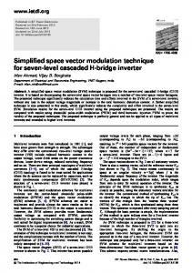
Nowadays, some applications as photovoltaic systems and switched reluctance machines are increasing their importance in the power arena. In this way, a new generation of singlephase power converters improving the efficiency and the reliability is needed. The power demand and the grid codes imposed by the governments lead to think on multilevel converters as a possible solution fulfilling all these requirements. Increasing the number of levels of the converters, the power and the quality of the output signals are improved. Since multilevel converters appeared, different topologies have been proposed [1-4]. Diode-clamped converters (DCC), Flying-Capacitor converters (FCC) and Cascade converters are the most common multilevel converter topologies presenting advantages or disadvantages in terms of minimum number of power devices, modularity and stability. Usually, these converters have been presented as three-phase converters but they can be adapted to work as single-phase converters. In [5], the most common multilevel single-phase converters are summarized considering that they are working driving a switched reluctance machine. In [6], single-phase converters are applied to small distributed power generation. All the possible switching configurations (named in this paper as state vectors) of single-phase multilevel converters are presented in [5]. For instance, a five-level single-phase DCC is shown in figure 1. Each leg of the power converter can be switched as it is shown in Table I obtaining three possible output phase voltages (0, ±E). As VAB is the output voltage of the single-phase converter and using (1), five possible voltages
(0, ±E, ±2E) can be achieved adding and subtracting the phase voltages of phase A and B.
VAB ã VA0 – VB 0
(1)
In this paper, single-phase multilevel converters are studied in order to design modulation methods improving some features as the number of commutations or the DC-Link voltage unbalance. II. MODULATION TECHNIQUES Different modulation methods can be used for single-phase multilevel converters adapting the three-phase modulation techniques. Carrier based Pulse Width Modulation (PWM) and Space Vector Modulation (SVM) methods for three-phase multilevel converters have been presented [6]. In the next points, carrier based PWM and SVM techniques for singlephase multilevel converters will be presented.
Fig. 1. Single-phase five-level DCC. TABLE I POSSIBLE SWITCHING CONFIGURATIONS FOR SINGLE -PHASE FIVE-LEVEL DCC Sb 4
Output Voltage VAB 0
Sa 1
Sa 2
Sa 3
Sa 4
Sb 1
Sb 2
Sb 3
off
off
on
on
off
off
on
on
off
off
on
on
off
on
on
off
-E
off
off
on
on
on
on
off
off
-2E
off off
on on
on on
off off
off off
off on
on on
on off
E 0
off
on
on
off
on
on
off
off
-E
on
on
off
off
off
off
on
on
2E
on
on
off
off
off
on
on
off
E
on
on
off
off
on
on
off
off
0
A. Carrier based PWM method Carrier based PWM technique is based on the obtaining of a pulse train where the pulses width has the modulation information. The simplest possible implementation of this modulation technique can be done using triangular carriers with frequency fc trying to modulate a reference signal (Vref) with lower frequency fs. In general, carrier based PWM techniques can be divided in unipolar and bipolar [7]. In figure 2, an example of level-shifted unipolar PWM modulation is shown. In the unipolar case, the control strategy generates only one reference voltage (Vref) to be modulated and, for N-level converters, N-1 triangular carriers (Ci) are used existing different modulation methods depending on the level (level-shifted method) or phase disposition (phase-shifted method)of the carriers [6][7]. The modulation strategy output is the modulated signal (MS) that has to be obtained from the converter. One external control has to decide the final switching of the power semiconductors to obtain those voltage levels because depending on the multilevel converter topology, different switching configurations obtain the same output voltage level. For instance, if a single-phase five-level DCC (see figure 1) is used, from Table I it can be seen that level 0 can be obtained from three different switching configurations. On the other hand, bipolar PWM techniques were presented in [7] where Vref and Vref are taken into account to generate the pulse train for phase A (MSA) and B (MSB) respectively. The external control also has to decide the switching of power semiconductors to obtain the desired output phase voltage levels. A bipolar PWM method for a five-level single-phase converter is shown in figure 3. B. Space Vector Modulation method The second most common modulation technique is the Space Vector Modulation (SVM) where the reference vector, generated by an external control strategy, is represented in a vectorial diagram and is composed as a linear combination of the possible state vectors of the power converter. Nearest Three Vectors (NTV) technique is normally used in three-phase systems determining the three nearest vectors to the reference one [8][9]. These vectors are used in the switching sequence to compose the reference vector and the duty cycles are calculated using geometric expressions. The control region of a power converter can be represented determining the phase voltage Vphase-0 for every possible switching configuration in each phase. For instance, in the five-level single-phase converter, each phase can obtain three different output levels. The control region of a single-phase five-level converter is shown in figure 4 where 2E is the DCLink voltage. The possible state vectors of the power converter are labeled using a couple of numbers SASB denoting the state of phase A and B respectively. This phase state is equal to zero if the lowest possible output phase voltage is achieved.
Fig. 2. Unipolar five-Level Level-shifted PWM technique.
Fig. 3. Bipolar five-Level PWM technique. Each pulse train is applied to each phase of the converter respectively.
In the five-level single-phase converter control region, nine possible state vectors appear and these are the unique possible voltages to be achieved when the converter is working. Other output voltages have to be obtained as linear combinations using one SVM method. As the output voltage of a singlephase converter is VAB voltage, it can be calculated for every combination of the state vectors using (1). In figure 5, VAB voltage of the five-level single-phase converter is shown. For instance, VAB equal to 1.7E, 0.55E and -0.85E are represented. It can be seen that different combinations of state vectors achieve the same output voltage VAB. In fact, there are different valid solutions to obtain the same output voltage VAB that form diagonal lines with 45º slope. This important property is shown in figures 5 and 6 representing one important redundancy in the power converter that can be used to improve some power converter features as the DC-Link voltage balance, the commutation losses, load current ripple, ..., etc. III. THE PROPOSED N2V-SVM METHOD The control region considering the output voltage VAB can be determined and, for instance, the single-phase five-level converter control region is represented in figure 7. A similar control region was presented in [10] for the two-level case. This way of representation will be very useful to develop the SVM method proposed in this paper.
VA0 20
E 21
22
-E 10
0 11
12
00
01 -E
02
E
VB0
Fig. 4. Control region of a single-phase five-level converter.
The redundancy property is clearly shown in figure 7 where different redundant state vectors achieve the same output voltage VAB and therefore are located exactly in the same position in the control region. The nine possible state vectors for the single-phase five-level converter can be divided in two large vectors (02 and 20), four medium vectors (01, 10, 21 and 12) and three zero vectors (00, 11 and 22). From figure 7, it is clear that in the multilevel single-phase case, the space vector modulation method can be named as Nearest Two Vectors (N2V) because only the two nearest state vectors to the reference one are needed in the switching sequence to generate the reference vector. The flow diagram of the proposed N2V-SVM technique is represented in figure 8. This method determines the switching sequence (formed by two space vectors) using geometrical properties where, among the possible redundant vectors, the state vectors with minimum voltage levels are used. For instance, if the modulation algorithm determines that state vectors 10 or 21 are present in the switching sequence, by default state vector 10 would be used. a=V ref /2E
a>0 NO
YES
statea1 =0 statea2 =0
stateb1=0 stateb2=0
a0.5
Fig. 5. Output voltage VAB for every linear combination of phase voltages in a single-phase five-level converter.
VA0 20
X
X
10
X
X
00
X
X
21
11
01
YES
NO YES
X 22
X
VB0 12
X 02
Fig. 6. Control region of a single-phase five-level converter. Different combinations of state vectors achieve the same output voltage.
Fig. 7. Control region for VAB for a single-phase five-level converter.
state b1=1 state b2=2 a=a+0.5 t 1=1+2a
state b1=0 state b2=1 t 1=1+2a
NO
state a1=1 state a2=0 t1=1-2a
statea1=2 statea2=1 a=a-0.5 t1=1-2a
Fig. 8. Proposed N2V-SVM algorithm for a single-phase five-level converter.
Once the N2V-SVM algorithm has been executed, one optimization strategy can be used in order to improve other features of the power converter using the redundancy property. These optimization algorithms define strategies to determine the best linear combination of state vectors to obtain the desired VAB voltage and, taking advantage of the redundancy property, improve some characteristic of the power converter. A. N2V-SVM balancing the DC-Link Voltage in DCC One possible optimization strategy can be based on reducing the DC-Link voltage unbalance of the single-phase DCC. In this way, the state vectors of the power converter affect to the voltage balance as it is shown in Table II where IAB is the load
current from A to B (see figure 1). It is assumed that an external device, i.e. a power rectifier is controlling the total DC-Link voltage making it approximately constant. From Table II, it is clear that large and zero state vectors do not create any unbalance in the DC-Link voltage and a possible solution for the modulation method to avoid unbalances is to use, among all the possible solutions to carry out the modulation, state vectors 20, 11 and 02. In fact, using these state vectors the five-level single-phase DCC is switched as a three-level single-phase converter because the possible output voltage VAB values in this case are 0 and ±2E. Therefore, this solution will not be considered.
TABLE III OPTIMIZATION STRATEGY TO CHOOSE THE REDUNDANT STATE VECTORS IN ORDER TO MINIMIZE THE DC-L INK UNBALANCE FOR A SINGLE-PHASE FIVELEVEL DCC Desired VAB Voltage -E
Redundant State Vectors 01-12
IAB0
IAB0
TABLE II VOLTAGE UNBALANCE FOR EVERY STATE VECTOR OF THE FIVE -LEVEL SINGLEPHASE DCC State Vectors 00 11 22
C1 voltage IAB>0 IAB