Design and Synthesis of Reversible Arithmetic and Logic Unit (ALU) Nor Syahira Mohd Mahayadin1, Lenin Gopal2, Adib Kabir Chowdhury3, Alpha Agape Gopalai4, Ashutosh Kumar Singh5 1,2,3,4
Department of Electrical & Computer Engineering, Curtin University, Malaysia 5 Department of Computer Application, NIT Kurukshetra, India E-mail:
[email protected]
Abstract –In low power circuit design, reversible computing has become one of the most efficient and prominent techniques in recent years. In this paper, reversible Arithmetic and Logic Unit (ALU) is designed to show its major implications on the Central Processing Unit (CPU).In this paper, two types of reversible ALU designs are proposed and verified using Altera Quartus II software. In the proposed designs, eight arithmetic and four logical operations are performed. In the proposed design 1, Peres Full Adder Gate (PFAG) is used in reversible ALU design and HNG gate is used as an adder logic circuit in the proposed ALU design 2. Both proposed designs are analysed and compared in terms of number of gates count, garbage output, quantum cost and propagation delay. The simulation results show that the proposed reversible ALU design 2 outperforms the proposed reversible ALU design 1 and conventional ALU design. Index Terms – reversible ALU design, reversible full adder, propagation delay.
I.
INTRODUCTION
For the past decades, there were numerous of difficulties and problems occurred in the development of conventional computing technologies. The major problem of the conventional computing technologies is power dissipation which is an important issue in today’s computer chip [1]. The advancement in Very Large Scale Integrated (VLSI) designs especially in portable device technologies lead to faster, smaller and more complex electronic system design [2]. In VLSI design, the conventional logic circuits dissipate more power. In the conventional logic circuits, every bit of information loss will generate kTlog2 joules of heat energy [3]. In the conventional logic circuit design, information loss occurs due to the total number of output signals is less than the total number of input signals applied to the logic circuit. Reversible computing is a promising method in low power dissipating circuit design for current technologies such as low power Complementary Metal Oxide Semiconductor (CMOS) design, cryptography, optical information processing, quantum computing and nanotechnology [4]. Reversible logic can be defined as thermodynamics of
information processing. Hence, it is used to reduce the power dissipation by preventing the loss on information. It is shown in[5, 6] that the circuit which designed using reversible logic can eliminate the heat dissipation due to information loss. This is due to the amount of energy dissipated in a system which bears a direct relationship to the number of bits erased during computation. The difference between the reversible circuits and conventional logic circuits is that the reversible circuits are built from reversible logic gates. Arithmetic and Logic Unit (ALU) works as a data processing unit which is an important part in the central process unit (CPU) of any computer architecture. ALU is a multi-functional circuit that performs one of a few possible functions on two operands and which depends on the control inputs [7]. ALU needs to continually perform during the life-time of any computational devices such as a computer or a hand held device such as hand phone. Thus, reversible logic can be implemented in designing ALU to reduce the power dissipation and propagation delay in the circuits [8]. In this paper, two new reversible ALU designs are proposed using two different reversible full adder logic circuits. In the proposed designs, eight arithmetic and four logical operations are performed. In the proposed reversible ALU design 1, Peres Full Adder Gate (PFAG) is used in the design, HNG gate [9] is used as an adder logic circuit in the proposed reversible ALU design 2. The proposed designs are analysed and compared in terms of number of gates count, garbage output, quantum cost and propagation delay. A short review on few existing reversible gates is detailed in section-II of the paper. Section-III introduces the proposed ALU designs. The simulations results are shown in section-IV where comparison between the existing ALU designs with the proposed architecture is presented and finally the paper is concluded in section-V. II.
REVERSIBLE LOGIC GATES
A reversible logic circuit is said to be reversible if the number of inputs is equal to the number of outputs [10]. In
order to achieve a synthesised low power circuit, the reversible logic circuits should have the following specifications which are minimum number of reversible gates or gate count, minimum number of garbage outputs, minimum propagation delay and minimum quantum cost [11]. In the proposed ALU designs, Feynman, Fredkin and Peres reversible gates are used in the proposed reversible ALU designs. The quantum implementations of the three gates are described in the following subsections. A. Feynman gate Feynman gate is also known as Controlled-Not gate (CNOT). It is a reversible of 2*2 gate with 2 inputs and 2 outputs. The quantum cost of Feynman gate is one. This is proven since it has mapping input of A and B to output of P and Q as shown in the Fig.1 [12]. Feynman gate is made from one EX-OR gate.
the outputs (P, Q, and R) and the quantum cost of the Peres gate is four. From the quantum implementation shown in Fig.3, Peres gate requires one V, two V+ and one CNOT gates. Peres gate is made from two EX-OR gate and one AND gate. III. PROPOSED ALU DESIGN ALU works as a data processing components which is an important part in the central process unit (CPU). Besides, it is the main performer in any computing devices. ALU is a multi-functional circuit that performs one of a few possible functions on two operands of A and B which is depending on the control inputs. A.
Conventional ALU Design
Fig.1: Quantum implementation of Feynman gate
B.
Fredkin gate
Fredkin gate is a reversible of 3*3 gate with 3 inputs and 3 outputs. The quantum implementation of the gate is shown in the Fig.2 that the inputs (A, B, C) are mapped to the outputs (P, Q, and R) and the quantum cost of Fredkin gate is five. The two dotted rectangles in the Fig. 2 is equivalent to a 2*2 Feynman gate with the quantum cost of one for each dotted rectangle. The other 3 quantum cost comes from one V and two CNOT gates [12].
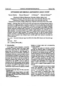
Fig.4: Block diagram of 1-bit conventional ALU design in Quartus II software
As show in Fig.4, the S2, S1 and S0 are the selection lines while Cin is the input carry. Input A and B are the data input for the ALU design. Based on the truth table shown in Table 1, when selection line S2 is equal to zero, the circuit performs eight arithmetic operations and when selection line S2 is equal to one, the circuit performs the logic operations of OR, EX-OR, AND and NOT functions. Table 1: Function table for ALU
Fig.2: Quantum implementation of Fredkin gate
C.
Peres gate
Fig.3: Quantum implementation of Peres gate
Peres gate is a reversible of 3*3 gate with three inputs and three outputs. The quantum implementation of the gate is shown in the Fig.3 that the inputs (A, B, C) are mapped to
S2
S1
S0
Cin
Operation
Function
0 0 0 0 0 0 0 0 1 1 1 1
0 0 0 0 1 1 1 1 0 0 0 0
0 0 1 1 0 0 1 1 0 0 1 1
0 1 0 1 0 1 0 1 X X X X
F=A F = A+1 F = A+B F = A+B+1 F = A+B’ F = A+B’+1 F = A-1 F=A F = A˅B F = A⊕B F = A^B F = A’
Transfer A Increment A Addition Add with carry Subtract with borrow Subtraction Decrement A Transfer A OR EX-OR AND NOT
Fig.4 is the logic circuit design for 1-bit conventional ALU which is implemented in Altera Quartus II software. 4-bits,
8-bits and 16-bits of conventional ALU design can be implemented by expanding 1-bit ALU design. B.
Reversible ALU
The proposed reversible ALU is designed to produce the same function as implemented by conventional ALU. Fig.5 is the block diagram of proposed reversible ALU designs. It has two main logic circuit design, namely, control unit and reversible full adder and the proposed design has five constants signals (e.g: Cinput1, Cinput2, Cinput3, Cinput4 and Cinput5) with a provision for realizing the eight arithmetic operations and four logic operations.
Fig.5: Block diagram of reversible ALU design
1) Control Unit Control unit is a critical part in the reversible ALU design. Control unit performs the arithmetic operations inside the ALU. As shown in Fig.6, the proposed control unit design is made up from three Feynman gates, three Peres gates and one Fredkin gate. Four control variables S2, S1, S0 and Cin select twelve different operations in the reversible ALU design. The arithmetic and logic operations are differentiated using the variable input of S 2. The control unit has four constant signals. There are eight garbage outputs in the proposed control unit logic circuit.
2) Reversible Full Adder Full adder is the important building block in ALU unit. Compatible reversible adder implementations is required in the anticipated paradigm shift logic compatible with the optical and quantum. The outputs of the reversible adder are given in the following equations: Sum=A⊕B⊕Cin
(1)
Cout= (A⊕B)Cin⊕AB
(2)
a) PFAGGate The PFAG gate is 4x4 reversible gate. Outputs, P and Q are considered as the garbage outputs. The output, R and S are represented the function of Sum and Cout respectively. The quantum cost of PFAG is 8 since it made from 2 Peres gates [13]. Fig.7 is the logic circuit design of PFAG gate in Quartus II software.
Fig.7: Logic circuit design of PFAG gate in Quartus II software
b) HNGGate The HNG gate is 4x4 reversible gate. Outputs, P and Q are considered as the garbage output. The outputs, R and S are represented the function of Sum and Cout respectively. The quantum cost of HNG gate is 6 [14]. Fig.8 is the logic circuit design of HNG gate in Quartus II software.
Fig.8: Logic circuit design of HNG gate in Quartus II sofware
3) Proposed Reversible ALU Design 1 Shown in Fig. 9 is the block diagram of the proposed reversible ALU design 1. The proposed ALU design is implemented in Altera Quartus II software which is show in Fig.10. Fig.6: Block diagram of control unit
Fig.12: Logic circuit design of proposed reversible ALU design 2 in Quartus II software.
IV.
SIMULATION RESULTS
Fig.9: Block diagram of the proposed reversible ALU design 1.
Shown in Fig.13 is the simulation in QSim waveform simulator for both reversible PFAG and HNG gates and the function of the adder circuits can be verified through the simulations.
Fig.10: Logic circuit design of proposed reversible ALU design 1 in Quartus II software.
4) Proposed Reversible ALU Design 2 Shown in Fig. 11 is the block diagram of the proposed reversible ALU design 2.
Fig.13: Simulation waveform for reversible full adder.
Shown in Fig.14 is the output simulation in QSim waveform simulator for both reversible ALU designs. The output simulations satisfy the function Table 1 for A=0 and B=1.
Fig.14: Simulation waveform for reversible ALU design. Fig.11: Block design of the proposed reversible ALU design 2
Shown in Fig.12 is the logic circuit design for 1-bit reversible ALU which is implemented in Quartus II software. 4-bits, 8-bits and 16-bits of reversible ALU design can be implemented from 1-bit ALU design.
Table 3 and Table 4 show the performance comparison of the conventional ALU design with the proposed reversible ALU designs. For comparison, number of gate count, garbage output, quantum cost, and propagation delay are considered as the performance matrices.
Table 3: Comparison between the proposed reversible ALU Design 1 and Design 2
Parameter which has to be compared Design 1: Control Unit + PFAG Design 2: Control Unit + HNG
Gate count 9
Garbage output 10
Quantum cost 28
8
10
26
Comparison of 2 Reversible ALU Design 50
28 26 9 8
10 10
Control Unit + PFAG
requirements of the reversible logic by having the low propagation delay. V.
CONCLUSION
In this paper, the reversible ALU design is proposed with two unique design paradigms. The proposed reversible ALU designs are verified using Altera Quartus II software. Both proposed designs are analysed and compared in terms of number of gates count, garbage output, quantum cost and propagation delay. The simulation results illustrate that the proposed reversible ALU design 2 outperforms the proposed reversible ALU design 1 and conventional ALU design. ACKNOWLEDGMENT
0
Control Unit + HNG
This work is fully funded by Ministry of Science, Technology and Innovation Grant Number 01-02-07SF0028 Malaysia. REFERENCES [1]
Fig.15: Comparison of 2 reversible ALU designs based on three parameters Table 4: Comparison of propagation delay between the conventional ALU and reversible ALU designs
Number of Bits
Propagation Delay (ns)
1-bit 4-bit 8-bit 16-bit
Reversible ALU Design 1 (ns) 7.75 8.38 8.79 7.39
Reversible ALU Design 2 (ns) 7.17 8.13 8.29 8.26
Conventional ALU (ns) 8.17 8.73 9.43 9.13
Comparison of Propagation Delay between Reversible and Conventional ALU Design 10
Design 1 (Reversible) Design 2 (Reversible) Conventional
5 0 1-bit
4-bit
[2]
[3]
[4]
[5] [6] [7]
[8]
[9]
8-bit 16-bit
Fig.16: Comparison of propagation delay between the conventional and reversible ALU designs
[10]
Table 3 shows the comparison between the proposed design 1 and design 2 of the reversible ALU. We can depict from the Fig. 15 that the proposed reversible ALU design 2 is better than the proposed reversible ALU design 1. Based on Table 4, the comparison on propagation delay between two designs of reversible ALU and the conventional ALU is made. Based on the result as shown in Fig. 16, we can conclude that the proposed reversible ALU design 2 shows higher reductions in propagation delay as compared to the proposed design 1. Hence, design 2 of reversible ALU is the best design compared to design 1 which meets the
[11]
[12]
[13]
[14]
R. H G, A. B. Suresh, and M. K N, "Design and Optimization of Reversible Multiplier Circuit," International Journal of Computer Applications, vol. 52, pp. 44-50, 2012. A. Dixit and V. Kapse, "Arithmetic & Logic Unit (ALU) Design using Reversible Control Unit," International Journal of Engineering and Innovative Technology, vol. 1, pp. 55-60, 2012. R. Landauer, "Irreversibility and Heat Generation in the Computational Process," IBM Journal of Research and Development, vol. 5, pp. 183-191, 1961. H. R. Bhagyalakshmi and M. K. Venkatesha, "An Improved Design of a Multiplier using Reversible Logic Gates," International Journal of Engineering Science and Technology, vol. 2, pp. 3838-845, 2010. C. H. Bennett, "Logical Reversibility of Computation," IBM Journal Research and Development, vol. 17, pp. 525-532, 1973. C. H. Bennett, "Notes on the History of Reversible Computation," IBM Journal of Research and Development, vol. 32, pp. 16-23, 1998. M. K. Thomsen, R. Gluck, and H. B. Axelsen, "Reversible Arithmetic Logic Unit for Quantum Arithemtic " Journal of Physics A: Mathematical and Theory, vol. 43, pp. 1-13, 2010. R. Saligram, S. S. Hegde, S. A. Kulkarni, H. R. Bhagyalakshmi, and M. K. Venkatesha, "Design of Parity Preserving Logic Based Fault Tolerant Reversible Arithmetic Logic Unit," International Journal of VLSI Design & Communication Systems, vol. 4, pp. 53-68, Jun 201. M. S. Sankhwar and R. Khatri, "Design of High Speed Low Power Reversible Logic Adder Using HNG gate," International Journal of Engineering Research and Applications, vol. 4, pp. 152-159, 2014. J. Kurian, L. A. Alex, and V. G, "Design and FPGA Implementation of a Low Power Arithmetic Logic Unit " IOSR Journal of VLSI and Signal Processing, vol. 2, pp. 57-61, 2013. A. A. Lakhsmi and G. Sudha, "Design of a Reversible Single Precision Floating Point Subtractor," Springer Open Journal, vol. 3, pp. 1-20, 2014. R. S. B, T. B G, and P. B, "Transistor Implementation of Reversible PRT Gates," International Journal of Engineering Science and Technology (IJEST), vol. 3, pp. 2289-2297, 2011. R. Garipelly, P. M. Kiran, and A. S. Kumar, "A Review on Reversible Logic Gates and Their Implementation," International Journal of Emerging Technology and Advanced Engineering, vol. 3, pp. 417423, 2013. R. A. H V, P. K. BV, and M. KN, "Design of Control Unit for Low Power ALU Using Reversible Logic," International Journal of Scientific & Engineering Research, vol. 2, pp. 1-7, 2011.