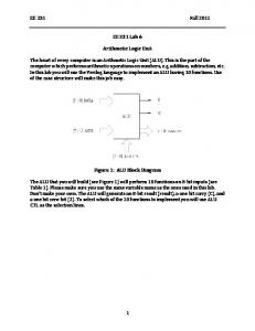
IET Circuits, Devices & Systems Research Article
Reconfigurable arithmetic logic unit designed with threshold logic gates
ISSN 1751-858X Received on 31st January 2018 Revised 11th April 2018 Accepted on 25th April 2018 doi: 10.1049/iet-cds.2018.0046 www.ietdl.org
A. Medina-Santiago1 , Mario Alfredo Reyes-Barranca2, Ignacio Algredo-Badillo1, Alfonso Martinez Cruz1, Kelsey Alejandra Ramírez Gutiérrez1, Adrián Eleazar Cortés-Barrón2 1Computer
Science Department, CONACYT-National Institute of Astrophysics, Optics and Electronics, Luis Enrique Erro No. 1, Tonatzintla, 72840 Puebla, Mexico 2Electrical Engineering Department, CINVESTAV-IPN, Ave. IPN No. 2508, Col. San Pedro Zacatenco, 07360 CDMX, Mexico E-mail:
[email protected]
Abstract: In recent years, there is a trend towards the development of reconfigurable circuits where devices using them offer flexibility and performance. Different technologies are explored, such as threshold logic gates (TLGs), which are one of the most promising future technologies, and researchers are examining and improving different characteristics such as density, performance and power dissipation. This research presents a 4-bit arithmetic logic unit (ALU), which was designed using TLGs through reconfigurable logic blocks with a universal circuit configured with three stages based on a floating-gate metal oxide semiconductor transistor with more than one control gate, which was named neu-complementary metal oxide semiconductor (νCMOS). The main contribution is that this device is configured as a ν-CMOS inverter and has the ability to program the threshold voltage of its transfer curve by applying an external voltage to the additional control gates. The number of input bits and the magnitude of the weighted input capacitances related to control gates of the ν-CMOS inverters is obtained and analyzed by using the graphical method (floating-gate potential diagram). Finally, the proposed 4-bit ALU shows similar results as those measured from the ALUs implemented in the field programmable gate array evaluation kit and the Motorola chip MC14581B.
1 Introduction Although threshold logic gates (TLGs) have been a research area covered since a long time ago, currently it is now considered that very-large-scale integration (VLSI) implementations are not still mature enough; several approximations for configurations that use capacitive, conductance/current or differential implementations can be found [1]. Also, reconfigurable [2–6] and not reconfigurable developments [7–9] based on TLGs are available. At present, it is considered that a reliable development of the threshold logic is being delayed since the TLG design is based on the full-custom design methodology and because there is lack of high-level synthesis tools [1, 10]. In general, the utility of TLGs as a design alternative will be determined not only by the availability of feasible basic blocks, costs and performance capacity but mainly by the existence of automated synthesis tools that can improve all its properties. For example, algorithms are being proposed as part of the research generated by the importance of TLG and its potential [11, 12]. In addition, theoretical and experimental efforts from particular advantages are being carried out, which were identified in the use of logical threshold circuits. Although there are still performance limitations, such as the static energy consumption, the fan capacity, the silicon area needed and the dispersion of the technological parameters, it could be anticipated that once these problems are solved, the design of the TLG circuit may be easy. In this way, contributions reported in [9, 13, 14] show proposals that are being executed to reinforce this logic design methodology. Reconfiguration is an additional property that can be found between different configurations that can be conceived with TLGs. This property can be achieved using the neu-complementary metal oxide semiconductor (ν-CMOS), which can be described as a multiple-input floating-gate (MIFG) metal oxide semiconductor field effect transistor (MOSFET). A MIFG is a circuit with multiple input gates, which are capacitively coupled to an electrically isolated floating gate. Besides, it has behaviour as a biological neuron to which several signals arrive and are processed to deliver an output based on an activation function. IET Circuits Devices Syst. © The Institution of Engineering and Technology 2018
Correspondingly, in the context of the ν-CMOS, a weighted sum of the voltage applied to each of the inputs in the floating gate is performed, controlling the state ON/OFF of the metal oxide semiconductor (MOS) transistor depending on the sum of voltage. Taking advantage of a well-established threshold level of the system, a TLG can be designed; this can lead to a basic circuit configuration that can perform all the Boolean functions based on programmable-bias inverters with external voltages, whose values depend, in particular, on the designed logic gate. A proper design process of the basic TLG configurations can develop reconfigurable circuits simplifying the number of devices used. A significant difference in the construction of logical functions consists of the number of devices used in TLG circuits compared with conventional gates as mentioned in [2]. Although ν-CMOS transistors are devices with high inherent capacitances, they are still an interesting option for reconfigurable circuits. Despite the problems encountered in the development of TLG circuits, this study proposes a design flow of an arithmetic logic unit (ALU) that uses reconfigurable basic blocks with an emphasis on the design process that can result in a digital system based on the ν-CMOS. This paper is organised as follows. In Section 2, we describe the ν-MOS technology, whereas, in Section 3, we present the floatinggate potential diagram (FPD) on which the design of the proposed ALU is based. In Section 3, the design methodology where a description is given for the basic blocks and the fcarry block is presented. The results obtained from the simulation using the proposed TLG ALU, the comparisons, where the ALU is implemented in both a field programmable gate array (FPGA) evaluation board and a commercial chip are given in Section 4. Finally, Section 5 draws the conclusions.
2 v-MOS technology The development of circuits began in the 1930s with the creation of the field-effect transistor, passing through the bipolar junction transistor (1947), until arriving at the CMOS [P-type MOS 1
Fig. 2 Block diagram of the basic configuration of a ν-CMOS TLG circuit Fig. 1 Topology of a MOS transistor with multiple control gates
(PMOS), N-type MOS (NMOS)], which was designed in 1960 and then used to implement integrated circuits (ICs). The MIFG νMOS transistors were developed in 1967 and applied since 1989 in the Electrically Erasable Programmable Read-Only Memory, reducing the number of interconnections on a chip. At the present time, conventional and commercial circuits are still being designed with CMOS, whereas the ν-MOS transistors are used in specific applications. Therefore, the MOSFET transistor is used in the construction of the circuit and can be of type P or N, which results in CMOS technology. This technology allows implementing different passive and active devices, whose dimensions are smaller than square micrometres in the same manufacturing process, and thus integrate them into a small silicon chip. The decision to integrate with CMOS technology is based on the cost and portability of the design. The trend of memories for neural networks is to use standard technologies such as the 1.2-micron double poly-silicon, which is very accessible. Floating-gate structures report several features such small areas, low power consumption and compatibility with standard technologies. The main challenge of the technology is to reach such scaling, where the area of ICs is optimised, achieving a compromise between the complexity of the circuits and the size of the chip. The floating-gate circuits and conventional MOS circuits have different characteristics. On the one hand, the conventional MOS transistors report: (i) CMOS inverters only have a maximum input for typical use, (ii) circuit arrangements performing a certain function require an area that depends on the number of components (more arrangements involve higher area), (iii) the CMOS inverter requires a small number of capacitances, (iv) the delay times in arrays (to analyse logic gates) have small values, and (v) frequency limits for arrays with these transistors (in logic gates) show high values (above 10 MHz). On the other hand, the reports of the logical ν-MOS present: (i) possibility of implementing multiple control gates such as inputs and feeding one, some or all of the inputs, (ii) advantage of saving transistors in digital circuits, (iii) disadvantage of greater number of capacitances, (iv) the delay times are greater and, consequently, (v) the frequency ranges are smaller. Fig. 1 shows a double-standard poly-silicon CMOS process, where there are three important points that should be considered when design circuits use ν-MOS transistors: (i) the devices must be discharged with ultraviolet light or other discharge techniques, which remove the residual values stored during manufacturing, (ii) there is a dependence between the drain and source current and the drain voltage of the ν-MOS device, which is more pronounced than in a standard MOSFET and can be minimised using additional techniques (aspect ratios or helmet-type devices), and (iii) the νMOS inverter is a standard block of multi-valued binary circuits, where this structure can consume static power depending on the state of the inputs. The important parameters for the design of the circuits, such as the native threshold voltage and the thickness of the oxide, depend on the used technology. In this case, these parameters occur in two situations: (i) poly-silicon 1 (poly I) and substrate (N-type material), and (ii) poly-silicon 1 (poly I) and poly-silicon 2 (poly II), see Fig. 1. Therefore, it is a primordial requirement to know in advance the respective values of the technology, in order to make the correct computations. In the ALU proposed in this work, the 2
technology is 1.2 μm in length of the channel, double metal, double poly-silicon and well N of AMI, whose parameters are shown in (1), more details in [15] V th(n) = 0.5154122 V, V th(p) = − 0.8476404 V,
(1)
tox(poly II − poly I) = 31.7 nm . Several lines of research in ν-MOS technology are being developed, for example, the work presented in [16] focuses on the loading and unloading times of the ν-MOS transistor, in other words, the injection and extraction of load of the floating gate, as well as the comparisons in power consumption, while in [17], technology that operates with millivolts is reported. In the proposed work, the 4-bit ALU based on TLG uses the 1.2-micron technology and operates at 3.3 V, this is due to the budget allocated for these designs within our institute, and the focus is not on the injection and extraction of load from the floating gate, but the number of transistors used in CMOS and ν-MOS technologies, obtaining significant reduction and high performance. Mainly, the design based on ν-MOS and TLG presents a drastic reduction in the number of transistors as well as interconnections when it is compared with conventional transistors. For example, a 3-bit A/D converter requires 16 ν-MOS transistors, while requiring 174 conventional CMOS transistors. The reduction in the number of transistors and their interconnections are some of the most studied problems in the design of VLSI logic circuits, for this reason, the floating-gate ν-MOS transistor is a device that reduces the processing time and derives the scalar product in a simple way with the storage of weight in neural networks.
3 Basic configuration and design flow A ν-CMOS transistor is the core of a TLG circuit and must be designed with several control gates that function as weighted inputs in each stage. Therefore, it is required to know the value of these capacitances to obtain the desired logical function. A graphical representation of each Boolean function can be drawn, where the voltage on the floating gate of the ν-CMOS is plotted as a function of a multi-valued input voltage, named V P, and mapped from a nbit digital input. The authors of [3, 18] showed that the number of programmable inverters, the respective applied external voltage, and the coupling capacitances (weighted) can be derived graphically from the frame called FPD. Logic functions such as AND, NAND, OR, NOR, XOR, and XNOR can be designed using a single basic configuration by applying the respective external voltages, see Fig. 2. The circuit is configured with three basic stages as follows: (a) pre-charge input stage consisting of a ν-CMOS inverter with six control gates and a common floating gate; (b) programmable inverter stage, which has five programmable ν-CMOS inverters with two control gates each, the latter as inputs, and (c) output νCMOS stage, where there is a ν-CMOS inverter with ten control gates. V P is the multi-valued input that depends on the digital inputs (4 bits) and counts as feeding the three stages. In Fig. 2, V P represents the input of four bits and is represented by an input to convert it IET Circuits Devices Syst. © The Institution of Engineering and Technology 2018
Fig. 4 Block diagram of a programmable inverter, where V P corresponds to the 4-bit input and V ext is the external voltage input V A to V E, corresponding to each used programmable inverter
Fig. 3 Theoretical FPD for the output ν-CMOS inverter. The case for the XOR gate is illustrated. Values for the coupling capacitances of are C1 = (15/32)γCTOT , CA = (3/32)γCTOT , CB = (2/32)γCTOT , CC = (4/32)γCTOT , CD = (3/32)γCTOT , CE = (3/32)γCTOT , and CF = (1/32)γCTOT
into a multi-valued signal only for simulation purposes. V C2 and V F are used in the first stage to adjust the appropriate output that is required from the pre-charge stage at the time it feeds the ν-CMOS inverter in the third stage for a given logic function. The second stage contains five programmable inverters, A, …, E, and has the purpose of establishing the transition of the respective inverter through the threshold level γV DD /2, which is shown in Fig. 3. Finally, C1, CA, …, CF representing the weighted inputs that feed the floating gate to trigger on the ν-CMOS inverter in the third stage; this is based on the truth table of the corresponding gate. An XOR gate function is used mainly in the proposed ALU, and Fig. 3 shows the corresponding FPD for the configuration presented in Fig. 2. As a 4-bit input is considered, the x-axis is divided into 16 subdivisions and the y-axis is divided into 32 subdivisions [19]. The threshold level is γV DD /2, where γ is the floating-gate gain and is expressed in (2), where CTOT is described in (3); the left y-axis represents the coupling capacitances of the final ν-CMOS stage and the right y-axis denotes the voltage range of the floating-gate potential ϕFG (0 to γV DD) γ=
C1 + CA + CB + CC + CD + CE + CF , CTOT
(2)
CTOT = C0 + C1 + CA + ⋯ + CF .
(3)
To operate properly, some design considerations are described: capacitors C1 and CF must be equal in the pre-charge and ν-CMOS outputs; also, where CON and COP are the gate capacitance of the NMOS and PMOS transistors, respectively; besides, the 4-bit digital input is considered with C1, as C1 = CX1 + CX2 + CX3 + CX4 .
(4)
Fig. 2 shows that the 4-bit input feeds the three configuration stages at the same time. In addition, Fig. 3 shows that the value selected for V DD in this design was 5 V, therefore this will be the maximum value reached by V P on the x−axis of the FPD for a logical input of ‘1111’. The logical output values of an XOR logic gate are represented by the bold solid line, where a logic 1 is presented at the output when ϕF > γV DD /2 and a logic 0 when ϕF < γV DD /2, as specified at the top of the plot. Moreover, by extrapolating each inclined line IET Circuits Devices Syst. © The Institution of Engineering and Technology 2018
to the capacitance axis, the magnitude of each coupling capacitance of the ν-CMOS, can be derived. The baseline represents the variation of the floating-gate potential of the ν-CMOS when the external voltage that feeds all the programmable inverters is zero. Finally, the extrapolation of each vertical line of ϕF in Fig. 3 will indicate the external voltage that should be applied to the corresponding programmable inverter (depending on the logic gate considered), either as an absolute voltage value or as a fraction of V DD in general. An FPD can be drawn for different logic gates by means of their corresponding coupling capacitances and external voltage values for the programmable inverters. Moreover, there is no established design standard for the coupling capacitance magnitude in the pre-charge stage, but in this work, it is proposed to follow the usual binary weight for each bit, that is, each input bit is C0 times the position of bit 2n, where n = 0, 1, 2, 3, for the present case. Therefore, CX1 = 20 ∗ CO, CX2 = 21 ∗ CO, 2 3 CX3 = 2 ∗ CO, and CX4 = 2 ∗ CO. Fig. 4 shows a schematic representation of a programmable inverter, where V P is the multi-valued input given by four weighted input bits represented by CINV, and V ext is the external voltage derived from the x-axis of Fig. 3, with their respective coupling capacitances, CV, specified in the left-hand y-axis. For instance, as can be seen in Fig. 3, for the XOR logic gate, inversions of logic 1 to logic 0 are found at 3/16VDD, 5/16VDD, 9/16VDD, 12/16VDD, and 15/16VDD. The external voltages applied to achieve XNOR, NOR, AND, NAND and OR gates can be consulted in [18] for V DD = 5 V. It is important to mention that at the output of the programmable inverters, conventional CMOS inverters are needed for signal regeneration [14].
4 TLG-ALU circuit design More details about the design procedure of the individual TLG are presented in [18]. This procedure was applied in the design of a basic ALU to demonstrate the viability of the operation of this approach. The basic cell of the ALU is based on a logic XOR gate, which is used as part of the necessary adder to implement the logic and arithmetic operations performed by TLG-ALU. The inputs to the adder are three 4-bit summands: A, B and the carry input Cin. The outputs of the full adder are F (sum) and G (carry out), respectively. The analysed output functions are the well-known expressions of an adder with three digital inputs, which are described as F(sum) = A ⊕ B ⊕ Cin,
(5)
G(carry out) = AB + (A ⊕ B)Cin .
(6)
Although only two arithmetic and two logic functions are analysed with this proposal, a variety of operations can be performed. In particular, the operations arbitrarily selected to be performed with this ALU are expressed as Logic: AB, A ⊕ B,
(7)
Arithmetic: A + B, AB − 1 .
(8)
The type of operation can be selected and also controlled with a 4bit input signal (S3, S2, S1, and S0) that will be shown later. To evaluate the performance of the TLG-ALU, the response obtained after of the simulation with ORCAD will be compared with an 3
4.2 Operational blocks f 1 and f 2 In addition to the XOR block of the proposed ALU, the TLG blocks must be added to obtain the desired logic and arithmetic functions expressed in (6) and (7). These blocks are used for the implementation of the function f 1 and the function f 2, establishing the following considerations: Block f 1 is used to implement the logic operation AB, whereas block f 2 is used to implement ‘0’ function so that the operation (AB) ⊕ 0 = AB can be performed as a previous partial logical operation before the Cn function can be completed. ii. Again, block f 1 is used to implement the logic operation (A ⊕ B), whereas block f 2 is used to implement the ‘0’ function as before to perform the logic operation (A ⊕ B) ⊕ 0 = (A ⊕ B). iii. For the proposed arithmetic operation A + B, block f 1 must enable the variable A, whereas f 2 must enable variable B, so that the operation A ⊕ B = A ⊕ B can be obtained. iv. Finally, for the arithmetic operation AB − 1, f 1 must enable the function AB and block f 2 must enable the function ‘1’, respectively, to complete the selected arithmetic operation AB ⊕ 1 = AB − 1. i.
Considering two 4-bit input variables (A and B), the blocks for XOR, f 1, f 2, and fcarry are interconnected as shown in Fig. 6 for a reconfigurable ALU. Each of the selected functions can be enabled using the selection bus S3, S2, S1, and S0 illustrated in Fig. 6 using the combinations shown in Tables 1 and 2. Here, the outputs X and Y are, in turn, the inputs to both, the XOR and fcarry blocks in Fig. 6. In the proposed circuit, there are two 4-bit variables; then four blocks have to be used in this design, one for each element of the input vector (0, 1, 2, 3). Next, the FPDs for f 1 and f 2 have to be plotted together with the logic output previously defined in Tables 1 and 2, respectively, so that the corresponding input weighted capacitances and transition levels of the programmable inverters used in each block can be graphically deduced to configure the operational blocks f 1 and f 2 used in the design of the TLG-ALU. Figs. 7 and 8 show the FPD graphs according to the outputs X and Y that are expressed in Tables 1 and 2 based on the function to be performed. In this way, values in columns X and Y are specified in the top of each plot, see Figs. 7 and 8, respectively. Table 3 summarises the operation of the ALU unit based on the selection key bits and presents the truth table of the circuit diagram shown in Fig. 6. 4.3 Sum carry block fcarry
Fig. 5 Schematic diagram of the universal circuit used for logic gates configured with TLG (a) Input of the pre-charge stage, (b) Programmable inverter, (c) ν-CMOS inverter
ALU synthesised by using: (i) the Spartan 3E evaluation kit from Xilinx and (ii) the ALU chip MC14581B from Motorola. 4.1 XOR circuit block Each block presented in the basic configuration of Fig. 2 is specifically substituted with the equivalent circuits presented in Fig. 5 for the TLG-ALU simulation. Here, voltage-controlled voltage sources are used to represent the floating gate voltage of the three previous stages on the ν-CMOS technology [18].
4
The element used in the configuration of the adder that handles the carry is represented by the truth table shown in Table 4. Inputs X and Y correspond to the output from blocks f 1 and f 2, respectively. Fig. 9 shows the corresponding FPD for the fcarry function of the adder, this graph plots all possible combinations for a 4-bit vector although the adder will have only three input bits: X, Y and Cin. Then, column fcarry from Table 4 is limited to the maximum digital count of ‘111’. Therefore, only the first half of Fig. 9 must be considered in the derivation of the coupling capacitances and the external voltages for programmable inverters. Reviewing Figs. 3, 7 and 8 it is observed that when the value of ϕFG is above the threshold line, the output of the ν-CMOS is a logic ‘1’; otherwise, the output is a logic ‘0’. 4.4 Results The proposed ALU can handle 24 × 24 = 256 different input combinations, and some arbitrarily-selected examples will be presented. However, the tests that cover all options, showed full functionality of arithmetic and logical operations of the TLG-ALU circuit. Then, the logical and arithmetic function outputs are shown only for some input combinations, as indicated in each operation. IET Circuits Devices Syst. © The Institution of Engineering and Technology 2018
Fig. 6 Proposed ALU using TLG (a) Top module, (b) Block diagram presenting main modules
Table 1 Selection of the operation in the block f 1 Selection bits S1 S0 0
0
0
1
1
0
1
1
A
Output X
Function
B
Input 0 0 1 1 0 0 1 1 0 0 1 1 0 0 1 1
0 1 0 1 0 1 0 1 0 1 0 1 0 1 0 1
0 0 0 1 0 1 0 1 0 0 1 1 1 0 0 1
AB
The frequency used for the characterisation was 826 kHz; the tests performed with higher frequencies showed some glitches in the TLG-ALU and this behaviour can occur due to the model used for the ν-CMOS and the large capacitances needed for coupling input signals to the floating gate. Despite the proper operation described with this methodology, there are still some issues that must be investigated and improved. For instance, the simulation results, although representative, depending on the model used for the ν-CMOS in TLG. The work is still being conducted concerning the floating-gate MOS transistors. Furthermore, although this design with large capacitances is needed, this disadvantage is compensated by the reduction in the
IET Circuits Devices Syst. © The Institution of Engineering and Technology 2018
A
B
A⊕B
number of devices required to set a function, compared with the number of transistors needed with conventional MOS devices. It is important to note that the main advantage and the main contribution is that a circuit can be improved for this type of TLG system due to its capability to be reconfigured towards some other logic or arithmetic functions. 4.5 Arithmetic operations In this section, two arithmetic operations are presented (A + B and AB − 1), where three implementations are shown on a chip, FPGA, and ν-CMOS. The presented results correspond to a single signal
5
Table 2 Selection of the operation in the block f 2 Selection bits S3 S2 0
0
0
1
1
0
1
1
A
Output Y
Function
B
Input 0 0 1 1 0 0 1 1 0 0 1 1 0 0 1 1
0 1 0 1 0 1 0 1 0 1 0 1 0 1 0 1
0 0 0 0 0 1 0 1 0 0 1 1 1 1 1 1
0
A
B
1
Fig. 7 FPD for block f 1; transitions of the programmable inverters for block f 1 must be present at 4/16VDD, 6/16V DD, 8/16V DD and 13/16V DD, and values for the coupling capacitances of block f 1 are C1 = (16/32)γCTOT , CA = (3/32)γCTOT , CB = (2/32)γCTOT , CC = (2/32)γCTOT , CD = (3/32)γCTOT , CE = (5/32)γCTOT , and CF = (1/32)γCTOT
window, specifically when A = [8, 9, 10, 11] while B = [0, …, 15] for each value of A. A + B: Fig. 10 shows the plot for this operation, first for the measured output to the soft-hardware logic (TLG-ALU), second for the FPGA implementation and, finally, for the Motorola chip. In the output signals presented for each arithmetic operation, F(0) corresponds to the least significant bit, and F(3) corresponds to the most significant bit. For the ALU implementations, these signals show execution with similar results. ii. AB − 1: This operation is implemented on the same three technologies. Fig. 11 shows the full test-signal window, where vectors A, B, and F are presented. It can be seen that the results are the same in the three cases, although SHL implementation presents a small number of spikes, which has a very small amplitude and can be easily smoothed by using filters.
i.
6
4.6 Logic operations In this section, two logic operations are described: (AB and A xnor B), where three implementations are shown in the chip, FPGA, and ν-CMOS. As described in the previous section, the same conditions of the test values are analysed. i.
AB: Fig. 12 shows how the similarity of the output of the three implementations. The dotted line indicates the period of the A test value, where B changes 16 different test values. For example, when A = 0b1010 and B = 0b1100, then output F = AB = A and B = 0b1000. ii. A xnor B: Finally, Fig. 13 shows the test vectors for the three implementations. In the same way, as in the previous operation, the dotted line indicates the period of the A test value, where B changes 16 different test values. For example, when A = 0b1010 and B = 0b0000, then output F = A xnor xnor xor B = 0b1010 0b0000 = not(0b1010 0b0000) = not(0b1010) = 0b0101, which can be compared and visualised in the graphic.
IET Circuits Devices Syst. © The Institution of Engineering and Technology 2018
Fig. 8 FPD for block f 2; only two transitions can be identified at 6/16VDD and 8/16VDD and five coupling capacitances with the following magnitudes: CF = (1/32)γCTOT , CA + CB = (5/32)γCTOT , CC = (2/32)γCTOT , CD = (3/32)γCTOT , and CE + CF = (6/32)γCTOT
Table 3 ALU functions based on the selection of the control signal 4-Bit control signal S3 S2 S1 S0 0 0
0 0
0 1
0 1
1 1
0 1
0 0
1 0
Table 4 Fcarry's truth table X+Y Y X Cin 0 0 0 0 1 1 1 1
0 0 1 1 0 0 1 1
0 1 0 1 0 1 0 1
0 1 1 0 1 0 0 1
A
fcarry 0 0 0 1 0 1 1 1
For comparison, a number of transistors are necessary, which depends strictly on the designed circuit (application) and the power dissipation depends on the voltage-power supply computed by (9) of the chip and the current flowing in each device, which is computed as
V SP =
βn / βp ∗ V thn + (V DD − V thp) . 1 + βn / βp
(9)
(10)
The physical implementation of the proposed ALU is shown in Figs. 14 and 15. The first presents the basic layout cell for the main components of the ALU: 4-bit adder, which contains fcarry and XOR blocks, see Fig. 14a, and f 1 and f 2 blocks, see Fig. 14b. Additionally, a diverse semiconductor material is used, which is listed in the down of the figure. Additionally, Fig. 15 presents the layout of the SHL circuit for the 4-bit ALU, where the input/output ports and the cell ν-CMOS are plotted. This is manufactured by MOSIS, which provides different implementation metrics and parameters, such as area, number of transistors, power dissipation, and so on. IET Circuits Devices Syst. © The Institution of Engineering and Technology 2018
Function B
AB A⊕B A+B AB − 1
4.7 Comparisons
βn βp (V − V thp − V sp)2 = (V sp − V thn)2, 2 DD 2
Input signal
Specifically, the number of transistors depends on the discrete design and the layout of the SHL circuit designed and manufactured in MOS technology, see Table 5. At this point, the νMOS is a multi-input floating gate transistor that has multiple control inputs (floating gate). This technology applied in systems with large scale integration drastically reduced the number of transistors; otherwise, the number of transistors in CMOS technology only has one input gate, making the CMOS design to have: (i) a greater number of transistors for integrated high-scale ICs, and (ii) a greater number of interconnections. For example, using the SHL technique, a full adder can be made using only 8 νMOS transistors while a design using conventional CMOS gates will use 50 transistors [3]. However, a drawback of the SHL implementations is the large capacitance created by the weighted inputs, which generate greater area and affect the speed of the logic. The number of transistors used for the SHL ALU 4-bit chip design is 112 transistors, where 30 transistors are used in the precharge stage, six transistors for each programmable inverter, and eight transistors in the neuron stage. Compared with the MC12581B chip that is designed with CMOS technology and has a density of 326 transistors, the proposed ALU has a reduction of 66%. The manufacturer, called MOSIS Service, produced the chip and generated the report containing the manufacturing results and measurements of the MOSIS test structures on each wafer of the fabrication lot, where the measurements on a selected wafer are similar by using parameters and simulations in the tool SPICE. The important results of this work are: (a) the frequency clock is 37.97 MHz at 5.0 V, (b) the power dissipation per gate of the transistor at the operating frequency is 1.57 μW/MHz/gate, (c) the number of transistors and power consumption, where the commercial chip uses 324 transistors with a power consumption of 200 mW, while the proposed circuit has 112 transistors and consumes 79.2 mW, that is, 66% less power because of the interconnection density, (d) number of pines is 40, (e) technology is SCNA with λ = 0.8, (f) the layout size is 2181 × 2181 μm, and (g) the SHL chip design area is 4.757 mm2.
7
Fig. 11 Execution of operation AB − 1 for the three ALU configurations Fig. 9 FPD for the adder block; transitions are located at 0/16VDD, 4/16VDD and 8/16VDD and the coupling capacitances should have the following ratios: CA = (3/32)γCTOT , CB = (2/32)γCTOT , and CC + CD + CE + CF = (11/32)γCTOT
Fig. 12 Output comparison for the three ALU configurations with the AB logic operation
Fig. 10 Output comparison for the three ALU configurations with the arithmetic operation A + B
In the proposed ALU, the overhead of the TLG is controlled by the sum of potential in the floating gate, in comparison with the conventionally designed MOSFETs, which strictly depends on the compensation stage. At first instance, from results in Table 6, it can be observed that the TLG are a feasible option for digital reconfigurable circuits, in spite of the limitations present in the performance of the ν-CMOS such as the frequency operation, power dissipation, and operation control signals. Future work must still be done in order to overcome these limitations. Recently, researchers are exploring different areas for reconfigurable solutions or floating-gate based solutions. For example, Pengjun et al. [20] report a neuron MOS transistor that controls the weighted sum of the multiple-input gate and capacitance coupling effect on the floating gate, which is used for a multiple-valued D/A and A/D converter. Moreover, Kim et al. [21] describe an IC design, integration, characterisation, and algorithmic development of an integrated floating gate programming system for a large-scale field-programmable analogue array. In the same way, Homayoun [22] presents a hybrid design to perform logical vanishing by employing non-volatile 8
Fig. 13 Execution of the operation A xnor B for the three ALU configurations
embedded memory cells, where a look-up-table based on logic components from simple NAND and NOR gates to an array of IET Circuits Devices Syst. © The Institution of Engineering and Technology 2018
Fig. 15 Layout of the SHL circuit for the 4-bit ALU
5 Conclusion Fig. 14 Layout of the basic cell ν-MOS and the control voltage for the (a) 4-Bit adder, which contains fcarry and XOR blocks, (b) f 1 and f 2 blocks
Table 5 Transistors used in the complete 4-bit SHL circuit Type of cell Number of Number of Total transistors by cells transistors cell pre-load circuit programmable inverter circuit ν-MOS circuit 4-bit SHL circuit ONLY floating gate transistor chip 4-bit SHL circuit ONLY floating gate transistor + CMOS
Table 6 Comparisons Implementation Freq., MHz SHL FPGA Spartan 3E
0.826 94.34
CHIP MC14581B
0.826
2 2
1 5
2 10
2 14
1 1
2 14
14
8
112
Number of transistors
Power dissipation, mW
112 100,000 logic gates close to 80,000 transistors 324
79.2 12
200
This research showed that TLG based on v-CMOS circuits are a viable option for reconfigurable circuits since their design offers a reduced number of transistors compared with conventional alternatives. The basic cells can be designed and used for a more complex system design, such as the ALU presented in this work. In addition, it is important to mention that the advantage of this design is that it can be designed considering different polarisation voltages, CMOS technologies and the use of the respective technological parameters. This is possible through the qualitative information obtained from the FPD. On the other hand, using the proposed methodology, we design and compare the proposed ALU with a ALU configured with a commercial chip and with an FPGA evaluation board. The results are completely consistent among the three designs, showing the feasibility of the methodology based on the floating gates of ν-CMOS. Also, a group of two logical operations and two arithmetic operations was shown, producing the same results as those obtained for the commercial chip and an FPGA evaluation board. This methodology can be considered global because the same design can be made for different technologies or circuit polarisation.
6 Acknowledgment Authors express their gratitude to CINVESTAV-IPN IE-SEES and the Mexican National Council for Science and Technology (CONACYT) for financing this work through the Research Project 882 named Development of Security Systems for Application on Automotive Industry in the Tlaxcala state.
7 References [1]
gates providing a complex MAC arithmetic unit, Advanced Encryption Standard engine and, ultimately, the entire processor is developed. In addition, in [23], the authors implement a 4-bit ALU, which is designed and simulated in standard 350 nm CMOS technology and its power consumption is about 120 mW, and the ALU proposed in our research reports 79.2 mW. Finally, there are other design approaches to provide reconfigurable circuits such as carbon nanotubes [24], silicon nanowires at layout level [25], silicon-germanium heterojunction bipolar transistor technology [26], photonics at silicon level and electrons [27]. They are specifically focused on the level of electronic mobility, charge densities, body effects, and mobility in the transistor conduction channel. IET Circuits Devices Syst. © The Institution of Engineering and Technology 2018
[2] [3] [4] [5] [6]
Lirigis, V., Dubrova, E.: ‘Evaluation and comparison of threshold logic gates’. Proc. 37th Int. Symp. on Multiple-Valued Logic (ISMVL'07), Oslo, Norway, 2007 Aoyama, K.: ‘Operating margin-oriented design methods for threshold element-based reconfigurable logic circuits realizing any symmetric function’, J. VLSI Signal Process., 2004, 38, pp. 157–171 Shibata, T., Ohmi, T.: ‘Neuron MOS binary-logic integrated circuits – part I: design fundamentals and soft-hardware-logic circuit implementation’, IEEE Trans. Electron Devices, 1993, 40, (3), pp. 570–576 Lashevsky, R., Takaara, K., Souma, M.: ‘The efficiency of neuron-MOS transistors in threshold logic’, Soft Comput., 1999, 3, (20), pp. 20–29. DOI: 10.1007/s005000050087 Tran, T., Rothenbuhler, A., Barney Smith, E. H, et al.: ‘Reconfigurable threshold logic gates using memristive devices’. IEEE Subthreshold Microelectronics Conf. (SubVT), Waltham, MA, USA, 2012 Aunet, S., Berg, Y., Naess, O., et al.: ‘Novel reconfigurable two-MOSFET UV-programmable floating-gate circuits for CARRY, NAND, NOR or
9
[7] [8] [9] [10] [11] [12] [13] [14] [15]
[16]
[17]
10
INVERT functions’. 8th IEEE Int. Conf. on Electronics, Circuits and Systems, Malta, vol. 2, 2001, pp. 581–584 Murthy, P.H.S.T., Chaitanya, K., Murali Krishna, M., et al.: ‘FTL based 4 stage CLA adder design with floating gates’, Int. J. Comput. Appl., 2011, 17, (6), pp. 1–5 Ozdemir, H., Kepkep, A., Pamir, B., et al.: ‘A capacitive threshold-logic gate’, IEEE J. Solid-State Circuits, 1996, 31, (8), pp. 1141–1150 Wuu, T. Y., Vrudhula, S. B. K.: ‘A design of a fast and area efficient multiinput Muller C-element’, IEEE Trans. Very Large Scale Integr. (VLSI) Syst., 1993, 1, (2), pp. 215–219 Beiu, V., Quintana, J. M., Avedillo, M. J.: ‘VLSI implementations of threshold logic – a comprehensive survey’, IEEE Trans. Neural Netw., 2003, 14, (5), pp. 1217–1243 Oliveira, A. L., Sangiovanni-Vincentelli, A.: ‘LSAT – an algorithm for the synthesis of two level threshold gate networks’. Proc. Int. Conf. on Computer Aided Design, Santa Clara, CA, USA, 1991 Gowda, T., Vrudhula, S, Konjevod, G.: ‘Combinational equivalence checking for threshold logic circuits’. Proc. 17th ACM Great Lakes Symp. on VLSI, Stresa-Lago, Maggiore, Italy, 2007 Luck, A., Jung, S., Brederlow, R., et al.: ‘On the design robustness of threshold logic gates using multi-input floating gate MOS transistors’, IEEE Trans. Electron Devices, 2000, 47, (6), pp. 1231–1240 Rodríguez-Villegas, E., Huertas, G., Avedillo, M. J., et al.: ‘A practical floating-gate Muller-C element using vMOS threshold gates’, IEEE Trans. Circuits Syst. II, Analog Digit. Signal Process., 2001, 48, (1), pp. 102–106 The MOSIS Integrated Circuit Fabrication Service.: ‘Vendor-independent, scalable rules (MOSIS SCMOS rules): MOSIS scalable CMOS (SCMOS)’. Whitepaper, The MOSIS Integrated Circuit Fabrication Service, CA, USA, 2009 Parsan, F. A., Smith, S. C.: ‘CMOS implementation of static threshold gates with hysteresis: a new approach’. 2012 IEEE/IFIP 20th Int. Conf. on VLSI and System-on-Chip (VLSI-SoC), Santa Cruz, CA, USA, 2012, pp. 41–45. DOI: 10.1109/VLSI-SoC.2012.7332074 He, Z., Fan, D.: ‘Energy efficient reconfigurable threshold logic circuit with spintronic devices’, IEEE Trans. Emerg. Top. Comput., 2017, 5, (2), pp. 223– 237. DOI: 10.1109/TETC.2016.2633966
[18] [19]
[20] [21] [22] [23] [24] [25]
[26] [27]
Reyes-Barranca, M.A., Medina-Santiago, A.: ‘Methodology for the design of a 4-bit soft-hardware-logic circuit based on neuron MOS transistors’, Int. J. Electron., 2008, 95, (6), pp. 517–530 Cortés-Barron, E. A., Reyes-Barranca, M. A., Flores-NavaL, M., et al.: ‘4-Bit arithmetic logic unit (ALU) based on neuron MOS transistors’. 9th Int. Conf. on Electrical Engineering Computing Science and Automatic Control (CCE), Mexico City, Mexico, 2012 Pengjun, W., Jingang, L., Jian, X.: ‘Application of neuron MOS in multiplevalued logic’, Neural Comput. Appl., 2008, 17, (2), pp. 139–143 Kim, S., Hasler, J, George, S.: ‘Integrated floating-gate programming environment for system-level ICs’, IEEE Trans. Very Large Scale Integr. (VLSI) Syst., 2016, 24, (6), pp. 2244–2252 Homayoun, H.: ‘Vanishable logic to enhance circuit security’, United States Patent Application 20170103236, April 2017 Yadav, P., Kumar, G., Gupta, S.: ‘Design and implementation of 4-bit arithmetic and logic unit chip with the constraint of power consumption’, IOSR J. Electron. Commun. Eng., 2014, 9, (3), pp. 36–43 O'Connor, I., Liu, J., Gaffiot, F., et al.: ‘CNTFET modeling and reconfigurable logic-circuit design’, IEEE Trans. Circuits Syst. I, Regul. Pap., 2007, 54, (11), pp. 2365–2379. DOI: 10.1109/TCSI.2007.907835 Trommer, J., Heinzig, A., Baldauf, T., et al.: ‘Functionality-enhanced logic gate design enabled by symmetrical reconfigurable silicon nanowire transistors’, IEEE Trans. Nanotechnol., 2015, 14, (4), pp. 689–698. DOI: 10.1109/TNANO.2015.2429893 LeRoy, M. R., Raman, S., Chu, M., et al.: ‘High-speed reconfigurable circuits for multirate systems in SiGe HBT technology’, Proc. IEEE, 2015, 103, (7), pp. 1181–1196. DOI: 10.1109/JPROC.2015.2434818 Berrettini, G., Simi, A., Malacarne, A., et al.: ‘Ultrafast integrable and reconfigurable XNOR, AND, NOR, and NOT photonic logic gate’, IEEE Photonics Technol. Lett., 2006, 18, (8), pp. 917–919. DOI: 10.1109/ LPT.2006.873570
IET Circuits Devices Syst. © The Institution of Engineering and Technology 2018