CMOS flash Analog-to-Digital Converter (ADC) using Section II introduces the modified flash ADC architecture. ..... The DNL of our proposed flash ADC is within.
A New Low Power Flash ADC Using Multiple-Selection Method Wen-Ta Lee, Po-Hsiang Huang, Yi-Zhen Liao and Yuh-Shyan Hwang Abstract - This paper presents new low power CMOS flash Analog-to-Digital Converter (ADC) using multiple-selection method. As an example of 6-bit flash ADC, we use three extra comparators in our design to divide the next stage into four sections and control the switches whether can proceed to the 4-bit modified flash ADC or not. We use multiple-selection method to let only one section of the 4-bit modified flash ADC is allowed to operate, which achieve the aim of the low power consumption. Simulation and experimental results show that this proposed 6-bit flash ADC consumes about 19.2mW at 800M sample/s with 3.3V supply voltage in TSMC 0.35gLm 2P4M process. Compared with the traditional flash ADC, this multiple-selection method can reduce about 80.3% in power consumption.
The remainder of this paper is organized as follows. Section II introduces the modified flash ADC architecture. In section mI[, a new power reduction technique using multiple-selection method is proposed to modify the traditional flash ADC. Section IV shows the new 6-bit modified flash ADC simulation results. Finally conclusion is given in section V.
l
VIN V MSB
I. INTRODUCTION With the rapid growth of modem communications and signal processing systems, handheld wireless computers and consumer electronics are becoming increasingly popular. Mixed-signal integrated circuits have a tendency in the design of system-on-chip (SOC) in recent years. To limit energy in a reasonable size battery, minimum power dissipation in the mixed-signal integrated circuits is necessary. The ADC plays an important role between analog and digital signals. The traditional flash ADC has the advantage with very high sampling frequency and high conversion data rate [1]-[3], but its chip area and power consumption will cost very large depend on its high resolution. One simple way to achieve low-power consumption with reduced complexity is to use two-step flash architectures [4]. This technique has been used extensively in the past. In traditional flash ADC architecture, it uses 2' resistors and 2n-1 comparators to convert an n-bit data. Fig. 1 shows an example of a traditional flash ADC architecture. All 2n-1 comparators are working in every clock cycle [5] and thus will cause high power consumption. To reduce the power consumption for flash ADC, we propose a multiple-selection design method to reduce the number of comparators. Compared with the traditional 6-bit flash ADC uses 63 comparators, our new proposed 6-bit modified flash ADC architecture only uses 27 comparators therefore has smaller size and lower power consumption. Wen-Ta Lee, Po-Usiang Huang, Yi-Zhen Liao and Yuh-Shyan Uwang are with the Institute of Computer and Communication,
National Taipei University of Technology, Taipei, Taiwan, R.O.C., E-mail: wte ,tteut
1-4244-0637-4/07/$20.OO ©C2007 IEEE
LSB
Fig. 1. A traditional flash ADC architecture
II. MODIFIED FLASH ADC ARCHITECTURE A. Comparator
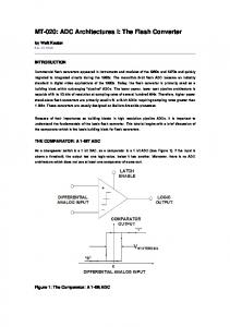
In any ADC, comparators are the most critical components because their input offset voltage, delay and input range directly influence the resolution and speed of the ADC. Furthermore, the noise generated within a comparator itself plays an important role in its overall performance at high frequencies. In order to reduce the power consumption, we use the high-speed low-power latched CMOS comparators shown in Fig 2. The comparator consists of a CMOS latch circuit and an S-R latch circuit [5]. When Vin > Vref, the output of V_,1 is high, and the output of VO11t! is low. On the contrast, when V111 < Vref, the output of V011t is low, and the output of V out! iS high. The outputs of comparators are used to control the switches, which are connected to the appropriate fractions of the reference voltage. Such a comparator is very important in the design of high-speed low-power ADCs, especially the modified flash ADC proposed in [6] or several other applications.
341
Authorized licensed use limited to: NATIONAL CHANGHUA UNIVERSITY OF EDUCATION. Downloaded on February 6, 2009 at 02:09 from IEEE Xplore. Restrictions apply.
VDD
Vbia
III. PROPOSED MULTIPLE-SELECTION FOR FLASH ADC
VDD
H
s
Vin | I D4=0 2:1
ISI_M_
Fig. 7, 8 show the HSPICE simulation results of our
proposed 6-bit flash ADC in TSMC 0.35Vtm 2P4M
Fig. 5. (a) A modified low-power 6-bit flash ADC (The first section output)
technology. The input ramp signal which voltage range is from 0 to 2V for proposed 6-bit flash ADC and the input sine-wave signal which operates at 1OMHz, the reference
Vref
t16u SI=1 SO=1 (Corn.)p=6)
i 3!4Vref Third 16
lI2Vref Second 16
voltage Vref= 2V, sampling clock rate at 800MHz and
S1
supply on 3.3V. The control signals (B5, B4) shows that the three extra comparators (Cl, C2, C3) can divide the next stage into four sections. These four sections are
I =a sh =o t 4-bit Modifie dFlah C3=0 J
4A1Iso
C2-11
=10l
power
D2
-
c1 D Sl=0SO=1p) 4-bitd M6hotlified Fhh C1 lX4
114Vref
First 16 t
1)
ModIwified1 Fla1h
4-bit
1,
|
/
D4=1
:
21
DO
4-bit
|
=
D5=
i
a=ornp=6 _ Modi11fiedFlash-
H gcamp
Fig. 5. (b) A modified low-power 6-bit flash ADC (The second section output) Vref 1p Furt 16 1 =SO=1 oapr) t| | 4-bit. ModifiedFlash J 3/4Vref *
|
=
s1o=npD2 4:1s M~odJifiedl Flmhi
Third 16
wo 4--bit
12Vref
Seconid16: t 14Vref II4Vref First 16
w
| SI=O SO=1 (c)=6)
4bit Modified Flh
|
Vref I 0=o=1
SIMULATION AND EXPERIMENTAL RESULTS
]
IV work
DO .o
-
_
/
D1 D5=o0
Xl
EN
*
=0
Si
j
Second 16 tco) M4\ITX 4-bit M\odified Flash Oo
EN
J I
=
Third 16
>
D
---_
LL--___
B2 ______
'l -
______
__i___L__I__I_ 1>
Bi
l
,
______
l iJjltIjLI BOLl I§;1 j1JIJll.Ij1jijijijL1jjj1 ]I I J L1 U[]j]lIJijLI1JIJij
(V) 0
200n
400n
600n
800n
lu(s)
Fig. 7. The simulation results of 6-bit flash ADC (Vin &=02 ramp signal)
Fig. 5. (d) A modified low-power 6-bit flash ADC (The fourth section output)
B
343 Authorized licensed use limited to: NATIONAL CHANGHUA UNIVERSITY OF EDUCATION. Downloaded on February 6, 2009 at 02:09 from IEEE Xplore. Restrictions apply.
__-----B-------------------------
----------------------------------
.3
____IHS
i
2
IVJIITLI
o
F1 f f
(V
~~~~~~~~~~~~_
----1-------------'-------
l -- --- --- ---f--- f-
]LiltITh i -0-HH-HH
i7Ifff
40n
80n
___
---
20n
o
B3
60n
1lOOn(s)
Fig. 8. The simulation results of 6-bit flash ADC (Vin 10lMHz sine wave)
Fig. 9. Layout of proposed 6-bit flash ADC
TABLE I
PAD- [JJJ [J[JJu PAD
+X
Comparison results of three different flash ADCs Analog---- -0-
~~\ |
Spec.
Te hno
\l
|
Power Supply
|Resolution
Traditional |Bi-section |Proposed Method Method Method TSMC/ |TSMC/ |TSMC/ ~0.35pim 0.35pim 0.35pim 3.3V 3.3V 3.3V 6 bits 6 bits 6 bits
|Input Anlo
02V
02
|
|68.3mW |19.2mW
Resolution
Technology | Power Supply | Reference Voltage Inu |Rag Input Range | Sample Rate | ~~INL I NL LD
6 bits
800MHz 0.4LSB/-0.8LSB 0 .-2LSB/ 0 --.7LSB
Power onsumpion
9.2mW
Chip-Area(-With-Pads)
1.131.13mm
2
I
PAD
Fi.1.Lyu
0
[2]
.
TSMC/0.3 5 im |3.3V |2V Ol2 0~~~~~~2V
113
fForpa
aotflopa
|REFERENCES M. Choi and A. A. Abidi, "A 6-b l.3-Gsamplels A/D of in 0.35-pm CMOS," IEEE JournalDec. Circuits, Vol. 36, No. 12, pp. 1847-1858, 2001. K. Uyttenhove and M. S. J. Steyaert, "A 1.8-V 6-bit ~~~~~~~~1.3-GHzflash ADC in 0.25prn CMOS," IEEE Journal of Solid-State Circuits, Vol. 38, No. 7, pp. 1115-1122, July
~~~~~~~~~[1] ~~~~~converter ~~~~~~~~Solid-State
TABLEIIII TABLE Specifications of proposed flash ADC |
LATCH nn nnr
|PAD
02V
|Consumption |97.5mW @800MHz
.
MUX4
IO_
T0.5/-0.3 |0.2/-0.7 |0.4/-0.6 |0.4/-0.8 |Fg
TT
IM IgI~ WL. LIZ13L
[ LIZ
|DNL(LSB) T 0.2/-0.3 |INL(LSB) |0.2/-0.3
Power
mUX
|2003.
P. C. S. Scholtens and M. Vertregt, "A 6-b 1.6-Gsamplels flash ADC in 0.18 pim CMOS using averaging termination," IEEE Journal of Solid-State Circuits, pp. ~1599-1 609, 2002. [4] Stojcevski. A., Singh. J., and Zayegh. A "Performance analysis of a CMOS analog to digital converter for telecommunications,". Proc.pp. IEEE ~~~~~~~wirelessConf |System ISIC-2001, Singapore, 59-62,Devices 2001. & [5] LE, H.P., Zayegh, A., and Singh, J. "A high-speed low-power CMOS comparator with 10-bits resolution,". Proc. 4th Int. Conf on Modeling and Simulation, MS'02, [3]
V. CONCLUSION
[6]
*
A new low-power architecture for a 6-bit CMOS flash ADC is presented. With the simulation results, our proposed multiple-selection method can save the power consumption about 80.30o than traditional method and
about 71.8°/O than bi-selection method. The DNL of our proposed flash ADC iS within 0.2LSB/-0.7LSB, the INL iS within 0.4LSB/-0.8LSB. The results approve proposed multiple-selection method can save the power
Melbourne, Australia, pp. 138-142, March 2003. flash Stojcevski. A., Singh. J., and Zayegh. A architecture with reduced power and complexity,". ~~~~~~~~~~~ADC Proc. 4th It. Conf on Modeling and Simulation, MS'02,
"'Modified
Melboume, Australia, pp. 169-173, 2002. Uyttenhove. K., Steyaert and M.S.J. "Speed-poweraccuracy tradeoff in high-speed CMOS ADCs," IEEE Trans. Circuits Syst. Il, Analog Digit Signal Process. pp. [8] 28-8,'02 1n =Chia-Chun Tsa, Kai-Wei Hong Yuh-Shyan Hwang, We-T Le an TogYnLe"Nwpersvg [7]
consumption for a CMOS flash ADC effectively.
design method for CMOS flash ADC," IEEE
International Midwest Symposium on Circuits and Systems, pp. t-371 - 1-374, 2004.
344 Authorized licensed use limited to: NATIONAL CHANGHUA UNIVERSITY OF EDUCATION. Downloaded on February 6, 2009 at 02:09 from IEEE Xplore. Restrictions apply.