Abstract. This paper presents a back-end design flow for high performance
asynchronous ASICs using single-track full- buffer (STFB) standard cells and
industry ...
High Performance Asynchronous ASIC Back-End Design Flow Using Single-Track Full-Buffer Standard Cells Marcos Ferretti, Recep O. Ozdag, Peter A. Beerel Department of Electrical Engineering Systems University of Southern California Los Angeles, CA 90089 – USA
[email protected],
[email protected],
[email protected] Abstract This paper presents a back-end design flow for high performance asynchronous ASICs using single-track fullbuffer (STFB) standard cells and industry standard CAD tools to perform schematic capture, simulation, layout, placement and routing. This flow is demonstrated and evaluated on a 64-bit asynchronous prefix adder and its test circuitry. The STFB standard cells provide low latency and fast cycle-times at the expense of some timing assumptions. This paper demonstrates that, by controlling top-block sizes and/or wire length within the place & route flow, ultra-high-performance circuits can be automatically designed. In particular, in the TSMC 0.25 µm process our post-layout STFB standard-cell 64-bit asynchronous prefix adder requires 0.96 mm2, offers a latency of 2.1 ns, has a throughput of 1.4 GHz, and operates at five process corners as well as a wide-range of temperatures and voltages.
1. Introduction As CMOS manufacturing technology scales into deep and ultra-deep sub-micron design, problems with clock skew, clock distribution, on-chip variations, and on-chip communication in high-speed synchronous designs are becoming increasingly difficult to overcome [1], warranting the exploration of alternative design approaches. In particular, asynchronous design is emerging as an increasingly viable alternative. Among the numerous asynchronous design styles being developed [3], template-based fine-grain pipelines have demonstrated very high performance [5][6][7][8][9]. Template-based approaches also have the advantage of removing the need for generating, optimizing, and verifying specifications for complex distributed controllers, which is both difficult and error-prone [2], the automation of which is an area of significant research [17]. Various templates tradeoff latency, cycle time, and robustness to timing. The most robust is the quasi-delayinsensitive (QDI) templates proposed by Lines [5]. One of
most aggressive is the ultra-high-speed GasP [7]. GasP offers high throughput but requires a bundled data design style that involves additional timing margins and assumptions that must be ensured and verified during physical design. In addition, the delay elements needed to address these timing assumptions often increase the forward latency of the blocks, which may significantly impact overall system performance. We recently proposed the single-track full-buffer (STFB) templates [10] which use 1-of-N data encoding to provide a practical tradeoff between performance and robustness. It uses twodimensional pipelining to achieve similar throughput to GasP with fewer timing assumptions and lower latency. In this paper, we propose a back-end design flow to support the automated design of STFB-based functional blocks and/or chips with standard commercial tools. In fact, to our knowledge, other back-end flows for templatebased fine-grain pipelines involve more labor-intensive semi-automated full-custom flows [18][19] or have adopted the use of existing low-performance standard cell libraries [20]. Moreover, our STFB library and the QDI library utilized in a high performance sequential decoder chip [21] are among the first standard-cell libraries for template-based designs that have been made available (through the MOSIS Educational Program) [22], allowing more widespread adoption of this technology. This paper demonstrates and evaluates this standardcell-based flow on a 64-bit asynchronous prefix adder and its test circuitry. In particular, in the TSMC 0.25 µm process our STFB standard-cell 64-bit asynchronous prefix adder requires 0.96 mm2, offers a latency of 2.1 ns and has a throughput of 1.4 GHz. Moreover, post-layout simulations show that it operates safely at five process corners as well as a wide-range of temperatures and voltages. The remainder of this paper is organized as follows. Section 2 reviews asynchronous channels and STFB templates. Section 3 presents details of the transistor-level design of the STFB cells. Section 4 describes the asynchronous library and ASIC design flows. Section 5 details the proposed test chip. Section 6 presents simulation results, Section 7 discusses area, cycle time,
Proceedings of the 10th International Symposium on Asynchronous Circuits and Systems (ASYNC’04) 1522-8681/04 $20.00 © 2004 IEEE
and latency comparisons with QDI and synchronous counterparts, and Section 8 draws some conclusions.
2. Background This section reviews asynchronous channels and introduces the single-track full-buffer (STFB) template.
2.1. Asynchronous Channels An asynchronous channel is a bundle of wires and a protocol to communicate data across the wires from one pipeline stage (the sender) to another one (the receiver). Figure 1 shows three different types of channels. The bundled-data channel has the advantage that the data is single-rail encoded (the same used in synchronous design) but is dependent on the timing assumption that the data is valid when the request signal is asserted. The request signal is typically driven through a delay line with a delay matched to the sender’s computation delay plus some margin. Alternatively, in a 1-of-N channel, the data (token) value is 1-of-N encoded where N wires are used to transmit N possible data values by asserting exactly one wire at a time. A blank or NULL is encoded by deasserting all wires. 1-of-2 (dual-rail) and 1-of-4 encodings are most common and both effectively use two wires per bit to encode the data.
resetting all the wires). The sender detects that the token was consumed before sending another token. Related designs include that from Berkel et al. [4] who proposed single-track handshake circuits to control medium-grain bundled-data pipelines. Sutherland et al. [7] later developed faster single-track GasP circuits to control fine-grain bundled-data pipelines. Nyström [8] also proposed a dual-rail (1-of-2) single-track template based on self-resetting pulsed-logic circuits like GasP but which requires significantly more transistors and is significantly slower. STFB templates, introduced in [10], offer GasP-like performance with template-based flexibility, allowing the utilization of conventional CAD tools.
2.2. STFB templates Figure 2 shows a typical STFB cell’s block diagram. When there is no token in the right channel (R) (the channel is empty), the Right environment Completion Detection block (RCD) asserts the “B” signal, enabling the processing of a next token. In this case, when the next token arrives at the left channel (L) it is processed lowering the state signal “S”, which creates an output token to the right channel (R) and causes the State Completion Detection block (SCD) to assert “A”, removing the token from the left channel through the Reset block. The presence of the output token on the right channel resets the “B” signal which activates the two PMOS transistors at the top of the N-stack, restoring “S”, and deactivates the NMOS transistor at the bottom of the N-stack, as shown in Figure 3, disabling the stage from firing while the output channel is busy.
Figure 1. Asynchronous channels. Figure 2. Typical STFB block diagram
In the 1-of-N channel, the receiver detects the presence of the token from the data itself and, once the data is no longer needed, it acknowledges the sender. In the typical four-phase protocol, the sender then removes the data by resetting all wires and waits for the acknowledgement to be de-asserted before sending another token. In the 1-of-N single-track channel, the receiver detects the presence of the token, as in the 1-of-N channel, but is also responsible for consuming it (by
Figure 3 shows a simplified schematic of the STFB dual-rail template. The NOR gate in this figure is the RCD, the NAND gate is the SCD and the NMOS transistor stack defines the cell’s main function. Note that the NMOS transistor stack is designed to be semi-weakconditioned in that it will not evaluate until all expected input tokens arrive [10]. The cycle time of the STFB template is 6 transitions and the forward latency is 2 transitions. This implies that
Proceedings of the 10th International Symposium on Asynchronous Circuits and Systems (ASYNC’04) 1522-8681/04 $20.00 © 2004 IEEE
the peak pipeline throughput can be achieved with just three stages per token, which allow the implementation of high performance small rings. The full-buffer characteristic of STFB stage refers to the capacity of each stage to hold up to one token.
Figure 3. Simplified dual-rail STFB template.
NMOS transistor width 0.6 µm and minimum PMOS transistor 1.4 µm. Also, we assumed, as a basis for the STFB cells creation, that the strength of the main N-stack should be, at least, twice of the minimum size NMOS. This means that the width of each NMOS transistor in the N-stack should be k*1.2 µm, where k is the number of transistors in the path to drive the state to ground. For example: for a 2 transistors path, the width of each Nstack transistor should be at least 2.4 µm. We use, for sizing, a known practical rule that one inverter can drive efficiently four to five times its own input load. By hand calculation we determined that, because the main N-stack has twice the strength of a minimum size inverter, it can safely drive a capacitance load equivalent to 20 µm of “gate width”, which is sufficient to drive the output transistor and the SCD as shown in Figure 3.
3.2. Balanced response
3. STFB Standard-Cell Design This section describes the transistor-level optimization implemented to improve performance and reliability in a standard-cell environment. Due to the timing assumptions in the STFB template, the transistor level design of each cell and sub-cell was done manually and checked through extensive SPICE simulation as described below.
Symmetrized transistor stacks are utilized to perform the SCD and RCD functions inside the cell. Figure 4 shows a 2-input NAND gate where the NMOS transistor stack of the conventional diagram is cut in the middle and symmetrized to allow the same time response for both inputs. This approach minimizes the data influence in the cell timing behavior.
3.1. Transistor sizing strategy An important characteristic of the STFB architecture is that all the channels are point-to-point channels. This means that there are no forked wires and the channel load is a function of the wire length and the next stage input capacitance. Consequently, since the fanout is always one, the variance on output load is even more dominated by the variation in the wire-lengths than is typical in synchronous designs. Therefore, our initial version of the library introduced here adopts a single-size strategy for each STFB function. The chosen size is reasonable to safely drive, with adequate performance, a buffer load through up to a 1 mm long wire with 0.4 µm width and 0.5 µm spacing. This implies that we can place and route a block as big as 0.5x0.5 mm with essentially no special routing constraints. Larger blocks can also be implemented as long as the wires are constrained to be smaller than this limit. Longer wires would result in poor transition times that could compromise timing assumptions and thus functionality. In the future, special CAD tools to automatically add STFB pipelined buffers within the P&R flow could also accommodate longer connections. Although the TSMC 0.25 µm process allows somewhat smaller transistors, we choose, as our minimum
Figure 4. Sub-cell NAND2B_28_12: (a) symbol, (b) conventional diagram and (c) implemented balanced input diagram.
3.3. Output sub-cell STFB_POUT The output driver sub-cell STFB_POUT is utilized in all STFB cells. It includes the staticizer structure and three PMOS transistors utilized to restore the state input (“S”) high as illustrated in Figure 5. If the output channel is empty, the “B” signal is high, “R” is low, and “NR” is high. During this time, M7 alone fights leakage and holds “S” high. At the same time, M2 and M3 hold “R” low. When “S” is driven low, the output driver PMOS transistor M1 drives the output “R” high, which makes the minimum size inverter drive “NR” low, deactivating M3 and activating M4 and M5. The RCD (not shown) will also make the “B” signal fall, activating M6. M4 will hold
Proceedings of the 10th International Symposium on Asynchronous Circuits and Systems (ASYNC’04) 1522-8681/04 $20.00 © 2004 IEEE
the line high while M5 and M6 drive “S” back high, turning off M1. Notice that M6 is controlled by the “B” signal from the RCD and its main function is to avoid any misfire caused by charge-sharing in the N-stack when a token is still present at the output (i.e., while the output channel is busy). Also, M5, which is controlled by the staticizer inverter (“NR” signal), is responsible to quickly assert “S” after firing.
is good enough to fight N-stack charge sharing) and by transistor sizing as shown in Figure 7, where the NMOS transistors of the balanced RCD are 1.2 µm wide, while, for a regular minimum sized NOR gate, we would use 0.6 µm.
Figure 7. (a) conventional 2-input NOR, (b) balanced RCD and (c) staticizer inverter.
3.5. Input channel reset transistors Figure 5. Sub-cell STFB_POUT (a) block diagram and (b) schematic.
This output stage topology offers a significant performance improvement allowing longer maximum wire length when compared with the initially proposed template [10]. It also improves robustness to charge sharing in the N-stack because this output sub-cell now has a lower switching threshold voltage.
3.4. The RCD sizing The NOR gate in the STFB template (RCD) is also implemented as a symmetrized gate and it is responsible to drive the “B” signal low no later than the signal “NR” goes low in order to disable the N-stack and restore the signal “S”, as shown in Figure 6. This is an internal timing constraint that needs to be met to avoid the shortcircuit current that would be caused by attempting to restore “S” while the N-stack is still enabled.
In the STFB template, the input token is consumed by driving the input channel wires low. It is done when the signal “A”, generated by the SCD block, activates a set of 5 µm wide NMOS transistors connected to each input wire. Also, to initially reset the entire circuitry, a global “/Reset” (active low reset) signal is used to force all channels low. Initially this signal was simply added as one input to the SCD block [10]. However, a 3-input NAND gate is much less efficient than a 2-input one. Figure 8.a shows the initially proposed 3-input SCD, where a 3-input NAND gate controls the reset transistors. Figure 8.b and c show the implemented reset structure, which uses 2-input NAND gates, allowing a smaller load on the states (“S0”, “S1”, “S2”) and offering a better performance of the SCD for dual-rail and 1-of-3 channels. Notice that the added transistors share the same drain connections, which results in a marginal increase in area and input capacitance for the STFB stage.
Figure 8. SCD and reset (a) initially proposed and the implemented (b) 1-of-2 and (c) 1-of-3.
3.6. Direct-path current analysis Figure 6. B and NR simultaneous activation.
This timing assumption is satisfied by reducing the load connected to the RCD output (WM6 = 0.6 µm, which
A perceived problem with STFB designs is the amount of direct-path current, also known as short-circuit current, caused by violations of the timing constraint associated with tri-stating a wire before the
Proceedings of the 10th International Symposium on Asynchronous Circuits and Systems (ASYNC’04) 1522-8681/04 $20.00 © 2004 IEEE
preceding/succeeding stage drives it. This section analyzes this constraint in detail. Figure 9 shows a conventional CMOS driver where both the PMOS and the NMOS transistor gates are connected together implementing an inverter. This means that during the rise (tr) and fall (tf) time of the input voltage (Vin) both transistors will be briefly active, allowing a direct-path current from VDD to ground. Since this current has an approximate triangular shape, we can estimate the direct-path current as Idp = Ipeak/2 [11].
SPICE simulation also showed that the direct-path current of the STFB templates is no worse than an inverter driving the line, and the timing assumption associated with tri-stating one stage before the other drives the line is not a hard constraint. For our STFB pipeline stages, the time difference between VA and VSx is bounded by the wire-length constraint to ensure correct operation.
Figure 9. (a) inverter and (b) direct-path current.
For our STFB pipeline stages, the NMOS transistor gate is connect to signal “A”, and the PMOS transistor gate is connected to “Sx” (one of the “states”). Figure 10 shows this implementation and the direct-path current if VA happens earlier than VSx. If the voltage difference (Vdiff = VA - VSx) is zero, the STFB stage Idp is similar to a conventional inverter. However, if one of the voltage transitions occurs ahead of the other, i.e., Vdiff is different than zero, we may observe a higher peak current during one transition and a smaller peak current during the next transition, or vice-versa.
Figure 10. (a) STFB output/input drivers and (b) directpath current if VA ≠ VSx.
Figure 11 shows the peak direct-path current versus the PMOS-NMOS gate voltage difference during an input rise/fall edge (Vdiff = VA - VSx). These values were obtained through DC Hspice simulation analysis using typical parameters with double than our minimum-sized transistors. Notice that, assuming that VA and VSx have the same shape (both have the same width, rise and fall times), the average peak current is not significantly different than the inverter peak current for Vdiff < 1 V. This means that a considerable difference between VA and VSx can be tolerated without a significant jump in power supply consumption.
Figure 11. Peak direct-path current versus the PMOSNMOS gate voltage difference.
4. Back-end design flow Here we describe the generation of the standard-cell asynchronous library and its utilization in the standardcell design flow.
4.1. Library design flow Figure 12 shows the design flow utilized for the creation of the STFB cell library. Each block is described below: Template specifications are the definitions of the utilized template as described in Section 3 and in [10]. Schematic, symbol and functional (Verilog) cell views are captured using Cadence Virtuoso environment and a text editor. Currently this step is done manually, however, synthesis from the template specifications is an area of future work. From the schematic, netlist SPICE files, that include automatically estimated source-drain geometries, based on gate widths, are generated for simulation and for LVS (Layout Versus Schematic check using Dracula), which, in turn, provides parasitic capacitance information and the source-drain geometries extracted from layout. Extensive Hspice simulations were used to verify the general operation and performance of all cells pre and postlayout. Schematic and symbol of frequently used sub-cell circuits were created to simplify and speed-up this phase, including a POUT sub-cell, various basic gates, and several common control cores for different numbers of inputs and outputs.
Proceedings of the 10th International Symposium on Asynchronous Circuits and Systems (ASYNC’04) 1522-8681/04 $20.00 © 2004 IEEE
Standard-cell specifications are the physical constraints utilized during the custom layout of the cell. For example, the cell height, power lines width, location of routing grid, etc. These are the same parameters utilized for synchronous cell designs and are necessary to make automated placement and routing feasible. Interestingly, the pins specifications needed to be in the grid and on a metal shape whose width is an even multiple of minor spacing grid steps (0.01 µm) to avoid off-grid error messages in the ASIC P&R phase.
the STFB library has been released [22]. It contains all common sub-cells for dual and 1-of-3 rail logic, cells for Buffers, Splits, Merges, BitBuckets, and BitGenerators as well specific cells used in our adder test chip. In the future, Verilog behavioral views of all cells will be completed and input capacitance and delay equations will be characterized and included in the library using the Liberty (.lib) file format [23].
4.2. STFB2_XOR2 cell example Figure 13 shows the layout of the STFB2_XOR2 cell. This cell is a STFB pipeline stage with two dual-rail input channels and one dual-rail output channel. In our library, this cell has four views: symbol, functional, schematic and layout. The symbol view is used to instantiate the cell in higher level schematics, the functional view is the verilog behavioral description of the cell, the schematic view has the transistor-level schematic of the cell, including the symbols of the sub-cells used to implement this cell, and the layout view, which, similarly to the schematic view, is composed of a cell-specific part and various sub-cells as shown in Figure 13. In this figure, we can see that the STFB2_XOR2 cell includes the 8 input transistors, that define the XOR function, and a STFB2_CORE4I sub-cell, which includes 4 reset transistors and one INV_28_12, one NAND2B_56_24, one NOR2B_14_12OD and two STFB_POUT sub-cells.
Figure 12. Standard-cell library design flow.
Layout & DRC are the manual physical design steps. To simplify this phase, reducing errors and saving time, sub-cell layouts were created matching the ones described in the schematic phase. Therefore, for most of the library cells, the top-level layout views are implemented with a mixture of sub-cells and cell-specific layout. The Diva Design Rule Checker (DRC) verifies that the layout satisfies all process design rules, however, it is also necessary to manually check if the cell complies with the standard-cell specifications mentioned above. Note also that the layout is done such that all cells DRCcleanly abut, even when horizontally and vertically flipped. An abstract layout view for the cells is generated using the Cadence tool Envisia Abstract Generator. The abstract file is in LEF format and represents the cells physical dimensions and the metal layers with a description of the power lines, input/output pins and metal obstructions. The placement and routing tool uses this file in the ASIC design flow. The resulting Asynchronous Cell Library is a tree of directories, for the Cadence tools, where the sub-levels are the cells, their views (symbol, schematic, functional and layout) and the abstract file. A preliminary version of
(a)
(b)
(c) Figure 13. STFB2_XOR2 cell layout (a) custom layout and STFB2_CORE4I sub-cell, (b) with STFB2_CORE4I sub-cell expanded, and (c) with all sub-cells expanded.
Proceedings of the 10th International Symposium on Asynchronous Circuits and Systems (ASYNC’04) 1522-8681/04 $20.00 © 2004 IEEE
Notice that, by re-arranging the input transistor connections shown in Figure 13.a, we can easily implement other two-input one-output cells such as STFB2_AND2 and STFB2_OR2.
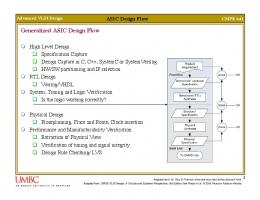
4.3. Asynchronous ASIC design flow Once we have STFB standard cells in our cell library, a conventional ASIC design flow can be utilized to generate a high performance asynchronous design as shown in Figure 14. Note that currently the entire design is entered through schematics (synthesis is an area of future work) and each block is sent to P&R and are then wired together in the chip assembly step. Verification can be performed through Verilog cell-level simulation and Nanosim transistor-level simulation.
g j = a jb j p j = a j ⊕ bj
0≤ j